The world over, countries are adopting the core elements of REACH, Europe’s three-year-old regulation on chemical use.
As the EC’s Environment Commission states, REACH aims to improve the protection of human health and the environment through the better and earlier identification of the intrinsic properties of chemical substances (http://ec.europa.eu/environment/chemicals/reach/reach_intro.htm). But what it says next is equally important: “At the same time, innovative capability and competitiveness of the EU chemicals industry should be enhanced” [italics mine].
Indeed, what REACH and its relatives around the world will necessarily create is such a bewildering maze of paperwork and fine print that they will act as de facto trade barriers. As Greg Dripps, Dow Electronic Materials’ global manager, Product Safety & Stewardship, noted recently, “Entry to markets will be slower.”
Speaking at the IPC Symposium on Electronics and the Environment in mid July, Dripps pegged the shifting worldview on chemical safety to the 2002 World Summit on Sustainable Development in Johannesburg, at which the concept of the precautionary principle was introduced. There, it was agreed to aim, by 2020, to use and produce chemicals in ways that minimize significant adverse effects on human health and the environment.
Certainly we’ve had fair warning of what was ahead. Fast forward to today, and the rising tide of substance regulation threatens to engulf us all. To wit:
South Korea is amending its Toxic Chemical Control Law, and moving toward a list of substances of very high concern (SVHC).
China is expanding the scope of its REACH-like list, going so far as to apply tests to chemicals under R&D – in other words, products for which there may not even be a market. Its scope will include all electronics equipment. However, self-declaration is permitted, and mandatory testing is no longer in effect. Stricter limits are ahead for wastewater and air emissions, although China has traditionally done a poor job of ensuring compliance.
Taiwan’s new chemical management program goes into effect next year, although some analysts, Dripps included, believe that deadline will slip.
Malaysia’s proposed laws closely resemble REACH, but implementation is being delayed.
Japan’s CSCL is migrating toward REACH, with phase-ins coming this year and next. Japan will ban some plating bath additives such as chromate and permanganate.
Canada’s “short list” has 4,300 substances on it, of which 500 are deemed “high priority.” Celestica supply chain management engineering consultant Kevin Weston says to plan on a 10-month lag for the government to respond to the submittal of chemical information.
In the US, laws vary by state. Nationally, the toothless 1976 Toxic Substances Control Act gives the Environmental Protection Agency authority to regulate and test chemicals that pose a health risk – but only for certain industries, and only when there is evidence of harm. In practice, just five chemicals have been restricted. It’s so weak, even the American Chemistry Council is lobbying to strengthen it. The new version requires safety determinations of several “expedited action chemicals,” including lead and Tetrabromobisphenol A (TBBPA), the flame retardant used in most laminate.
This, of course, means millions of chemicals and mixtures. My own SVHC (shortlist of very high concerns) is just how, exactly, we are going to collect and register all these data. Just knowing which companies are obligated to report information is a nightmare. (Hint: It’s not just the original chemical manufacturers. In fact, in some cases, distributors could be on the hook.) According to Kathleen Roberts, executive director of the North American Metals Council, under the Inventory Update Rule, there’s a reporting deadline of Sept. 30, 2011, for any chemical used this year. (Forms may be downloaded from the EPA website.)
The fundamental shift is not just the extent of substances to track. Rather, it’s the philosophical change that chemicals are guilty until proven innocent. Given the enormous difficulty chemical engineers have in separating the effects of one substance from others in its working environment, I can’t imagine how this will be accomplished.
Individual companies already are feeling pressure from down the supply chain. In researching solutions, I came across Actio (actio.net), a New Hampshire-based company that has developed sophisticated software for organizing and managing material safety data sheets, and cross-checking them against the latest global regulations. Jabil, for one, is now rolling out some of the Actio modules across its entire enterprise.
It couldn’t come at a better time. One major materials supplier to bare board fabricators told me he receives at least one request a day, often from customers in China, to cross-check their products against a regulated substances list. The checklists can contain up to 2,500 chemicals. Oh, and by the way, the company does not maintain an electronics database; it keeps a binder. (This is probably what Dripps had in mind when he noted the market barrier.) It’s enough to send employees jumping off every workplace roof, not just Foxconn’s.
There’s a silver lining. If they try, it will solve the US unemployment issue.
Mike Buetow is editor-in-chief of CIRCUITS ASSEMBLY; This email address is being protected from spambots. You need JavaScript enabled to view it..
Be aware that heavy parts are prone to falling off during soldering.
As automation becomes more prevalent and sophisticated in electronics manufacturing, plated through-hole designs are being phased out. PTH requires manual assembly labor that is less cost-effective than automated SMT methods, and is not feasible when dealing with ultra fine-pitch devices. That said, many designs still mix PTH and SMT. PTH also remains in use for some heavy power connectors, transformers, and other devices where strong mechanical bonds are required. Here we outline key best practices for double-sided, mixed-technology design.
K.I.S.S. Keep it SMT simple! On double-sided mixed boards, the solder side should be kept simple, meaning:
Discrete components wherever possible.
No fine-pitch devices or ball grid arrays.
Component height not more than 6 mm.
Manufacturing problems arise when components on the solder side of a mixed board are too heavy. If the board is assembled using a solder reflow pass for each side, heavy SMT parts attached to the solder side during the first pass may fall off during the second pass.
The general rule of thumb is, if the component is more massive than a PLCC-44, it will not hang on by surface tension. Said more technically, the mass to solder pad surface area ratio for such devices should be lower than 4.5 gm/cm2.
The solder side of a double-sided mixed-tech board may also be soldered by wave solder if the design permits. Using only discrete devices on the solder side and avoiding BGAs and fine pitch components keeps this option open. Solder joint formation using wave solder techniques is much more likely with these types of devices.
“Submarining” is a term used to describe the difficulties encountered when the leading edge of a board passes under the top of the wave on the wave machine. Solder will run down the top side of the card and essentially render it scrap. Very large panels with improper support are prone to sag in the wave solder preheat and any previous reflow cycles. This can increase the chances of a submarine.
Keeping a clear space around the edges of the board permits use of snap-on titanium stiffeners. These increase the rigidity of the panel and help prevent such occurrences.
Snap it. Another manufacturing design technique to observe is use of snap-off materials on the edges of the board. As mentioned, titanium stiffeners can then be used to help make the board more rigid. It also permits the panel to be handled smoothly in conveying and clamping systems. A 0.200" clearance is adequate, but nothing (not even fiducial keepout areas) should be placed in this zone.
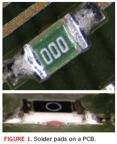
Pad it. Pad dimensions should be carefully considered on the bottom-side SMT of a double-sided mixed board. This includes extra thieving pads for wave-soldered ICs and extended toe pads to facilitate solder wicking. Both can significantly improve the yield at wave soldering (Figure 1).
In addition, components on the board should be oriented so that the solder joints are not shadowed as the board moves through the wave solder.
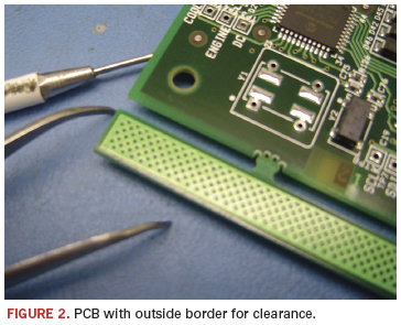
Clear it. If a double-sided mixed board is so dense that the above guidelines cannot be observed, a special fixture called a selective wave fixture (also known as a pallet) into which the board is snapped can be used. This masks the bottom-side surface mount from exposure to the wave. To do this, there must be sufficient clearance (0.1") between the PTH and SMT lands on the solder side so that the SMT can be masked by the fixture (Figure 2).
Keep in mind that fixtures add cost to the product; several fixtures are required, at several hundreds of dollars per fixture, and they have to be cleaned, loaded, unloaded and occasionally replaced.
Think single-sided. Overall, when designing a mixed board (using SMT and PTH), it pays to think single-sided! If possible, PTH parts should be placed on the same side of the board as the primary SMT devices. Double-sided PTH or PTH on the wrong side is almost certain to require manual soldering. There is just no other way to process them cost-effectively with existing automation.
George Henning is vice president of manufacturing at OCM Manufacturing (ocmmanufacturing.com); This email address is being protected from spambots. You need JavaScript enabled to view it..
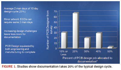
Dedicated tools help reduce the once-manual job by 20% of the typical design cycle time.
The question posted to the DesignerCouncil email forum was simple and straightforward: “Why on earth can’t these companies make a product out of the box that does engineering documentation well? I find it hard to believe there can’t be a boilerplate level delivered that could handle 80 to 90% of most companies’ documentation needs out of the box. … Even the BoM reports delivered out of the box from Oracle are absolutely useless. You need an integration company or an internal team of Oracle experts to spend a fair amount of effort just to get a usable BoM report.”
What’s fascinating, if not somewhat predictable, is how many firms take software that is intended (and good) at one function and repurpose it for something else. Take, for example, two of the best-known product life management tools: Oracle’s PLM and PTC’s Windchill. Good programs, both, but they were never intended to handle circuit board documentation. It’s one reason why it takes, on average, two man-days of the typical 10-day design cycle to complete the documentation (Figure 1).
Best-in-class processes reduce the amount of time spent creating the documentation; are automated so as to create a “living” document, or one that’s not fixed in time, unlike a paper printout of a pdf where, in the event of an engineering change order, the documentation needs to be regenerated; and facilitates product flow to the extent that the end-product quality is enhanced. As Downstream Technologies cofounder Joe Clark says, “Documentation is much bigger than just design, fab and assembly.”
Designers are pros at stretching the limits of CAD tools and other software, but at some point the deficiencies become too glaring to tolerate.
It’s why I’m surprised more haven’t turned to BluePrint, which purports to solve the headaches by providing access to all the electrical intelligence contained in the PCB CAD database to create detailed documentation in reportedly a far shorter timeframe than using traditional ECAD or MCAD tools.
The brainchild of DownStream, BluePrint was developed by former board designers who understand from firsthand experience the pains of their ex-colleagues. It uses a drawing- and sheet-based approach to create actual PCB documents (drill drawing, assembly drawing, parts list, and so on), and stores them in a digital release file. BluePrint uses the CAD data to automatically create unlimited views, details, and charts of the PCB, and can revise the documentation to reflect new PCB changes, reportedly in seconds. It’s not just a tool change; it’s a change in methodology.
Like MCAD, BluePrint can document drafting and dimensional specifications. Where BluePrint separates itself from the traditional MCAD tools, however, is in the number of required translations. Mechanical tools aren’t designed for the specific nature of a printed circuit board. To wit: MCAD cannot distinguish between a layer on a circuit board and a floor of a building. Meanwhile, BluePrint is a full 2-D drafting tool designed specifically to create PCB documentation and capable of creating anything that the CAD, fabrication and assembly departments might need. It eliminates constraints imposed by the PCB design tool for documentation, but retains the intelligence lost when using an MCAD tool for documentation.
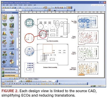
The best example of this is BluePrint’s support of unlimited PCB design views on any drawing sheet. Each instance of the design can be set with different display settings, scaling and formatting. However, each is also linked to the source CAD to automate ECOs, requiring one file translation from the source PCB CAD data to BluePrint (Figure 2).
As our emailer suggested, most users try to generate documentation from their ECAD tool. But ECAD was never intended for that purpose: Dimensioning is the domain of mechanical design. In practice, it’s another story. Asserts Clark, “Users do [documentation] in ECAD because they need to get it onto the piece of paper. There are lots of things done in the electrical design process that have nothing to do with electrical design; it’s all aimed at the documentation.” For instance, the use of assembly variants or mechanical components, which are never simulated but are pushed into a design capture or PCB layout tool to ensure they are represented in the final bill of materials.
BluePrint was developed to work with existing EDA tools. The MS Office environment requires a single load of the entire PCB CAD database to start the documentation process, and uses all the CAD intelligence to help create the documentation. ECOs are added by “refreshing” the source CAD data. BluePrint refreshes the documentation package, adding the new data in every instance of a board view, detail and chart.
“BluePrint brings ECAD design into the documentation tool,” says Clark. There, in the gallery (also known as the library, the term “gallery” is used so as not to be confused with the data for the PCB packages and land patterns), users create a drawing sheet, dragging and dropping the elements onto it. Any element – the number of zones, the font, colors, format, and so on – that is dragged and dropped on a sheet is “intelligent”; links remain active from the underlying design database, so if the links change, everything within the drawing is updated.
Inside the file are contained via stackup and drill layer pairs; drill symbols, patterns and charts; notes and callouts; mechanical component support; parts lists and assembly drawings; tooling, and so on. Schematic, Gerber, DFX, PDFs, plus any graphic or audio files are all stored. Or, in the words of Rick Almeida, DownStream’s cofounder, president and a former designer, “Any data used to create documentation and drive manufacturing.”
Automation of documentation is created by first creating the graphical “pictorial” of how the user wants to see a specific documentation element, for example, a “Via Stack-Up.” The graphical instruction defines how the via stackup should look. The via stackup could be amended, and the template modified to company-specific versions and saved for reuse. The template graphics are linked to data fields that pull the correct information from the PCB CAD data to intelligently create a via stackup that reflects the design intent and remains linked to the CAD data, so when the CAD data are updated (e.g., new layers or via ranges added or deleted) the detail is also automatically updated. “Essentially we use the same approach that is found in MS Excel chart build, where empirical data are married to user-specific graphics,” says Almeida. This same process goes for drill charts, parts lists, finger chamfers, coordinate lists, exploded views, etc.
BluePrint supports automation of the assembly drawing as well. This includes parts lists, which, even if not shown in the documentation set, are in the underlying design database and can be referenced as needed. The search function can find specific parts and component outlines. What it is not is a bill of materials management tool. “The parts list is a key part of the documentation,” explains Clark. “Documentation affects the parts lists, because as designers do the layout, they add mechanical parts, such as face plates, screws, washers. They need to be able to add to the parts lists and export them to the right department so they can add to the BoM and bring in all the attributes of the parts.” With BluePrint, users can import an external parts list from PLM or other enterprise systems, and sync the parts list with the assembly document, then export the parts list back to the enterprise system for ongoing management.
BluePrint follows the orientation of the board to place component reference designators. (The latter can be hyperlinked, too.) Assembly variants can be created at both the parts list level and also with a graphical assembly pictorial, with special legends to show what’s been installed, uninstalled or substituted. Documents such as relevant standards can be inserted as hyperlinks into the database. It also can generate rework sheets, showing cuts and jumpers, and include installation procedures.
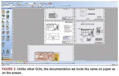
One complaint about reference designators in Oracle and SAP is that they do not display all instances of a particular part number with the part number and description in a single screen or menu. That’s not an issue for BluePrint. The documentation set in the GUI looks just as it will print on paper (Figure 3). The documentation package also can be exported as a pdf and posted to the Web, or as html on a company Intranet.
“It treats the end-product like a PCB, not a generic widget,” Clark says. “We don’t know how good our documentation is until we print it. Then, if something is wrong, we need to go back upstream and fix the ECAD database, then print again. What we do is allow the user to work with the documentation as it will be delivered upon release. This is a full 2-D drafting tool; it’s not intended to replace the mechanical group, but you need to be able to move and place things when doing the documentation. The handcuffs need to be removed.”
As we reported several months ago, Qualcomm has become one of the largest companies yet to standardize on BluePrint. Come this time next year, I would expect many more such announcements – and far fewer plaintive missives like the one at the beginning of this story.
Mike Buetow is editor in chief of PCD&F/CIRCUITS ASSEMBLY; This email address is being protected from spambots. You need JavaScript enabled to view it..
From QFNs to DFNs to MLPs, these packages are cheap, but tricky.
What are bottom termination components? You may not know the term “BTC,” but because IPC is focusing on these packages, expect to hear more about them. IPC has coined the term BTCs for descriptive package names such as QFN, DFN, SON, LGA, MLP, etc. They are in some ways similar to BGAs, which also have hidden terminations, but they are also very different. They do not have balls, but rather, metalized terminations or pads underneath the package.
Most, but not all, BTC packages have a large ground or power termination surrounded by smaller signal terminations. When it comes to inspection, they pose even more challenges than BGAs, which permit inspection by endoscopes. You may not be able to see side solder fillets, and even when you can, they may look non-wetted or dewetted. But, dewetted and non-wetted side fillets in BTCs are acceptable.
BTCs provide good electrical and thermal performance, and they are the cheapest package on the market. However, they do require perfection – not only in the assembly processes, but perfection on the part of the PCB and component suppliers as well, which need to supply flat PCBs and packages.
Guess the chances of getting perfect PCBs and packages: not likely. Through-hole components have been in use for more than half a century, but are still far from perfect, so don’t expect to achieve nirvana when it comes to this latest package trend.
The basic driver for BTCs is cost, which to a cost-competitive industry should come as no surprise. It is a package with the lowest per-pin cost, as low as half a cent per pin. To put this in perspective, if a package costs less than one cent per pin, it is considered a very low cost package. Thus, it is easy to imagine the attraction of this package, especially if the application is high volume such as cellphones or other mobile products.
Designers love this package because there are no leads, making BTCs an excellent choice as a result of their very low resistance and capacitance – also known as parasitic loss. Heat transfer from the package to the PCBs is also excellent, due to their large thermal pad in direct contact with the PCBs.
But there is no room for error. With no leads or balls, they must be perfectly flat, and the PCB must also be flat. How often does that happen?
The only variable the user has is solder thickness paste. However, if too much solder paste is used to compensate for package and PCB warpage, the package will float and may be misaligned. Also, expect excessive voids with too much paste.
If too little solder paste is used, and if there is any warpage in the package or PCB, expect many opens. There are difficult choices to make in the process selection, and inspection doesn’t help, since the end of the visible terminations are bare copper; hence, do not expect them to solder to achieve side fillets.
This is the reason why IPC has stepped in to help the industry develop a design and assembly guideline for BTCs. This author co-chaired IPC-7093, Design and Assembly Process Implementation for Bottom Termination SMT Components. The document describes the design and assembly challenges for implementing bottom termination surface mount components whose external connections consist of metalized terminations that are an integral part of the component body. The focus is on critical design, assembly, inspection, repair, and reliability issues associated with BTCs.
The target audiences are managers, design and process engineers, and operators and technicians who deal with the electronic design, assembly, inspection, and repair processes. The intent is to provide useful and practical information to those companies using or considering SnPb, Pb-free or other forms of interconnection processes for assembly of BTC-type components.
This document, although not a complete recipe, identifies many of the characteristics that influence the successful implementation of robust and reliable assembly processes, and provides guidance to component suppliers regarding issues being faced in the assembly process.
The exchange of information between the component supplier, product design, and assembly personnel about those parameters that influence good assembly practices is more critical with BTC implementation than with any other surface mount part.
During IPC Apex this year, committee members voted to accept the document pending minor revisions and final editing at a meeting to be held Aug. 31. We hope to complete deliberations Sept. 2, and plan to publish the document by the end of September.
Ray Prasad is author of Surface Mount Technology: Principles and Practice, and founder of the Ray Prasad Consultancy Group; This email address is being protected from spambots. You need JavaScript enabled to view it.. He will teach SMT-BGA-BTC Design and Manufacturing and Lead-free Implementation courses in Portland Oct. 11 to 13.
Simply recreating the PCB information adds steps, but little else.
Assigning I/O pins has transgressed well beyond a sketch or spreadsheet, and routing these large devices requires collaboration between FPGA and PCB designers. With modern I/O routing tools, savings can be realized in layer count, trace length (and consequential signal integrity improvement), and via use.
A good starting point is automation of symbol creation and PCB schematic connectivity to streamline the FPGA pin assignment process. Designers need to proceed with caution and investigate how such automation tools affect the complete product design flow. For example, an approximate recreation of the PCB information for use by an FPGA I/O assignment tool simply adds another step and another representation of the data – without fostering design convergence. Tools that create a unique set of product-specific symbol fractures for each FPGA design should be weighed against the company’s reuse and library management goals. Recreation of an entire local symbol and schematic set with each iterated pin change can make design a data management nightmare.
Instead, an FPGA/PCB optimization process that is the same from project-to-project focuses on a centralized library structure that promotes common practices among designs, as well as design reuse. Setting up this corporate “generic” environment that creates a true FPGA/PCB symbol theme has many downstream benefits, and also allows pin reassignments to be instantly communicated in a “push-button” fashion to all members of the design team.
At the librarian level, initially all symbol fractures for an FPGA are automatically generated, tied to the physical cell and part number, installed into a centralized library, approved, and made available for all users of the FPGA. FPGA power, ground, and config pins essential to the FPGA are optimally defined by the librarian, allowing functional designers to focus efforts on optimizing the I/O pins specific to the design. This approach not only fosters reuse, but avoids further design-specific regeneration of the symbol set for each iteration.
The upfront library configuration pays off not only in reusability, but also the ease through which pin iteration steps are completed. When a pin assignment change is made to the FPGA in the board context through the FPGA optimization tool, schematics containing the symbol set for the FPGA are updated with new connectivity information, and the centralized symbols themselves remain unchanged. This ease of iteration lessens the impact of design changes late in the design cycle.
To close the design loop, optimized pinouts are written and conveyed back in the FPGA vendor’s constraints file format – where the flow was initiated – as the signal names for the functional schematic, and initial pin assignments were obtained from the HDL and constraints file. Vendor I/O rules are followed throughout the process in the I/O optimization tool to adhere to DRCs for drive strength limits, VREF, I/O banking restrictions, LVDS proximity restrictions, differential pair recognition, and allowable I/O standard settings per pin. Vendor rules must be accurate and up-to-date and require close cooperation with suppliers to gain access to new architectures and package types.
From a physical implementation standpoint, comprehensive FPGA-to-PCB optimization requires further insight into the physical BGA implementation to be truly effective. Algorithms that unravel the pin connections on the FPGA to other components in the PCB context need to consider if BGA breakout and escape pre-routes have been utilized, as these effectively change the pin ordering. In the I/O optimization tool, unraveling the rats-nest connection to the escape trace endpoints provides shorter trace lengths, fewer PCB vias, and a more routable PCB than unraveling only to the pins.
Analyzing the entire design process may show that some solutions end up adding time and effort to the current project, or because the designs cannot be readily reused, future designs do not benefit as much. Optimization of connectivity meeting both FPGA and PCB design constraints requires tools that are PCB- and FPGA-aware (as well as BGA-aware), promote FPGA–PCB design concurrency while instituting repeatable processes, and have centralized reusable device representations.
Frank Smetana is market development manager at Mentor Graphics (mentor.com); This email address is being protected from spambots. You need JavaScript enabled to view it..
Every month between publication cycles, I try to reach out to designers to find out how things are going, what they working on, and of course, to find out if anybody has acquired any cool new guitars. Last week I talked to a friend (my twin brother of a different mother) many readers may know: Kelly Dack. Kelly works for IGT in Reno, NV. Not only does Kelly get to enjoy working and living in one of the most fantastic areas of the US, he and his colleagues at ITG get to work on some interesting boards. Those colorful and musical machines you see at any casino? ITG designs and builds them. If you’ve been to a casino lately, you may have noticed the flashing and pulsing lights that accompany the siren songs are changing. They are migrating to LED technology. According to Kelly, even the enticing sign that welcomes people to Reno is now lit by LEDs.
To people like me who have retired from daily board designing, LEDs were always a small part of our designs. They were employed to alert you whether the computer was on, or the car engine needed an oil change or something like that. Today, LEDs are at the heart of a dramatic change in energy conservation. They are no longer the little “ON” lights: They are the illumination for everything. Kelly and others have told me about boards chock full of LEDs. But there are issues with these boards with which more designers are going to have to contend and find answers.
From what I hear, a big issue right now is thermal management. When you put a bunch of LEDs on a single board, the heat buildup can be so significant as to cause failures. Some people are using heat sinks, bus bars and fans, of course. But going forward there will have to be better solutions. Metal core boards may be one answer, but other creative solutions are going to be required. I’ve heard that people are experimenting with cutouts in the substrate to get more direct contact with a metal core.
Another problem is one of capability and capacity on the manufacturing side. As reported by Mike Buetow, our manufacturing and business guru, only 15% to 20% of the EMS companies have production experience with metal core boards. As we all know, it does no good to design “it” if “it” can’t be manufactured at a reasonable cost and delivery. And then there is the issue of component traceability. Different LEDs have different light-emitting properties that are denoted by a “bin” code. Bin codes might be mixed on a board to get the right amount of light out. As such, assemblers have to track (scan) by serial number the LEDs on each board to ensure the end-product is to specification. They can’t simply swap one part for another, making tracking more complicated than with traditional passives.
It’s always interesting to see a new technology, or technology used in a new way. It’s one of the things that keep our jobs challenging. Expect to see more about the design and manufacture of LED boards in upcoming issues of this magazine and on our websites. In fact, for the first time, we have a class on LED board technology at PCB West (pcbwest.com) this year.
Speaking of PCB West (a somewhat transparent segue to set up a blatant plug), things are starting to heat up. As I write this, in early August, we are about seven weeks away from the annual trade show. Our VP of sales and marketing, Frances Stewart (known to some as She Who Must Be Obeyed), tells me that the show floor is just about sold out, and she is determined it will be full by the time we see you at the show. Registration is tracking ahead of this time last year, and we are looking forward to talking with a lot of people we haven’t seen in a while.
Space doesn’t allow me to list all the classes, but I do want to call your attention to a session on Wednesday called Designers’ Roundtable. This will be a somewhat free-form networking session to find out what designers are struggling with and share some ideas. We tried the Designers’ Roundtable at PCB Atlanta last year and the response was fantastic. According to designers and fabricators here in the Atlanta area, there is still a desire to have a better networking solution for designers. For whatever reason, most local Designers Council chapters haven’t met in some time. (I hear the same comments from a lot of local chapters.) I’d like to hear your comments about this at the roundtable and will be glad to share some of our thoughts as well.
In the meantime, stay in touch.
Pete Waddell is design technical editor of PCD&F; This email address is being protected from spambots. You need JavaScript enabled to view it..