Be aware that heavy parts are prone to falling off during soldering.
As automation becomes more prevalent and sophisticated in electronics manufacturing, plated through-hole designs are being phased out. PTH requires manual assembly labor that is less cost-effective than automated SMT methods, and is not feasible when dealing with ultra fine-pitch devices. That said, many designs still mix PTH and SMT. PTH also remains in use for some heavy power connectors, transformers, and other devices where strong mechanical bonds are required.
Here we outline key best practices for double-sided, mixed-technology design.
K.I.S.S. Keep it SMT simple! On double-sided mixed boards, the solder side should be kept simple, meaning:
- Discrete components wherever possible.
- No fine-pitch devices or ball grid arrays.
- Component height not more than 6 mm.
Manufacturing problems arise when components on the solder side of a mixed board are too heavy. If the board is assembled using a solder reflow pass for each side, heavy SMT parts attached to the solder side during the first pass may fall off during the second pass.
The general rule of thumb is, if the component is more massive than a PLCC-44, it will not hang on by surface tension. Said more technically, the mass to solder pad surface area ratio for such devices should be lower than 4.5 gm/cm2.
The solder side of a double-sided mixed-tech board may also be soldered by wave solder if the design permits. Using only discrete devices on the solder side and avoiding BGAs and fine pitch components keeps this option open. Solder joint formation using wave solder techniques is much more likely with these types of devices.
“Submarining” is a term used to describe the difficulties encountered when the leading edge of a board passes under the top of the wave on the wave machine. Solder will run down the top side of the card and essentially render it scrap. Very large panels with improper support are prone to sag in the wave solder preheat and any previous reflow cycles. This can increase the chances of a submarine.
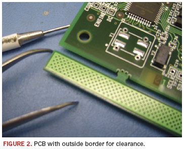
Keeping a clear space around the edges of the board permits use of snap-on titanium stiffeners. These increase the rigidity of the panel and help prevent such occurrences.
Snap it. Another manufacturing design technique to observe is use of snap-off materials on the edges of the board. As mentioned, titanium stiffeners can then be used to help make the board more rigid. It also permits the panel to be handled smoothly in conveying and clamping systems. A 0.200" clearance is adequate, but nothing (not even fiducial keepout areas) should be placed in this zone.
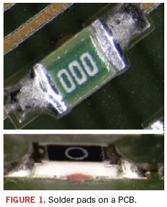
Pad it. Pad dimensions should be carefully considered on the bottom-side SMT of a double-sided mixed board. This includes extra thieving pads for wave-soldered ICs and extended toe pads to facilitate solder wicking. Both can significantly improve the yield at wave soldering (Figure 1).

In addition, components on the board should be oriented so that the solder joints are not shadowed as the board moves through the wave solder.
Clear it. If a double-sided mixed board is so dense that the above guidelines cannot be observed, a special fixture called a selective wave fixture (also known as a pallet) into which the board is snapped can be used. This masks the bottom-side surface mount from exposure to the wave. To do this, there must be sufficient clearance (0.1") between the PTH and SMT lands on the solder side so that the SMT can be masked by the fixture (Figure 2).

Keep in mind that fixtures add cost to the product; several fixtures are required, at several hundreds of dollars per fixture, and they have to be cleaned, loaded, unloaded and occasionally replaced.
Think single-sided. Overall, when designing a mixed board (using SMT and PTH), it pays to think single-sided! If possible, PTH parts should be placed on the same side of the board as the primary SMT devices. Double-sided PTH or PTH on the wrong side is almost certain to require manual soldering. There is just no other way to process them cost-effectively with existing automation.
George Henning is vice president of manufacturing at OCM Manufacturing (ocmmanufacturing.com); This email address is being protected from spambots. You need JavaScript enabled to view it..


