“All of us learn to write in the second grade. Most of us go on to bigger and better things.” – Bobby Knight
Well, they say that if you wait long enough, everything comes back around. After much soul searching, gnashing of teeth and a healthy dose of general anesthesia, I’ve decided to jump back into the PCD&F editor’s chair. To be honest, it’s the place and job title I’ve enjoyed most during the time I’ve been associated with this fine publication.
In the last few months, I’ve been talking to some of the folks in the PCB design and fab industry, trying to find out what I’ve missed and what has changed in my misspent years with other ventures and other job titles that lured me from you. Not that I’ve been totally out of touch – just that I haven’t been as close as I once was. According to the folks who would take my calls, the main things that have changed are all of the features are smaller (duh!) and high-speed has become more mainstream. Oh yeah, and the definition of high-speed has evolved by a factor of about a googleplex. There are new packages that my old, worn-out, permanently gridded eyeballs can barely see – but hasn’t that always been the evolution in electronics?
I’m not saying that I’d challenge anybody out there to a Top Gun (www.pcbwest.com/topgun/index.shtml) design-off, but I have yet to come up with any earth-shattering changes to this industry. It’s all evolutionary. Yeah, processes in fab have changed in the ever-continuing effort to keep up with design, and so have materials, test strategies and assembly equipment.
But having said that, last month, I had the opportunity to look at some cutting-edge designs. For the last 15 years or so, I’ve been involved with Mentor Graphics’ Technology Leadership Awards as a judge, looking at plots of boards and studying stats and the challenges these designers face. It is truly awesome to see some of the results.
Mentor has been sponsoring the TLAs for about 15 years now, and they deserve a pat on the back for doing this. They make a big deal out of focusing a spotlight on designers and acknowledging the difficulties designers face. Recently, UPMG joined Mentor Graphics in presenting a webinar announcing the winners of the 2009 Technology Leadership Awards. Support your fellow designers by viewing the event on-demand. You don’t have to be a Mentor user, just a person who appreciates good design work.
I enjoy the TLAs for multiple reasons. For one thing, I can still tell when and where someone “hand” routed the busses and where they used an autorouter. While I acknowledge the speed and cost benefits of autorouting, the old designer in me still thrills to the artistic side of our science. The truth is, some of these boards just have too many rules and too many constraints to not use an autorouter. The non-designer types here at UPMG think I’m wiggin’ when we look at a board, and I try to show them where the designer used his or her skill or struggled to get in those last 100 traces. Some of the innovation and creativity really blows me away when I look at these boards. You people are really smart and exceptional. I just wish that more EDA companies would do something similar to recognize designers.
I can’t get away without mentioning that PCB Atlanta is October 22 at the Alpharetta Marriott. It is one of our regional shows, really a scaled down version of the PCB Design Conferences. Go to www.pcbshows.com to check it out. If you are within traveling distance, register for the show and come see us. While you’re there, look for the TLA webinar.
And last but not least, we’ve started a blog page on pcdandf.com. Back Page fans will find this the closest thing to the original and can add their comments, criticisms and various contributions to the cause.
Sure, some things change, but it almost feels like getting back together with an ex-wife or girlfriend (here we go again). You’re familiar with certain and fundamental traits, but at the same time, there is no telling where either of you has been. All that aside, I’m glad to be back.
The demand for signal integrity engineers is on the rise, but universities have made slow progress in training for today’s power and signal integrity challenges.
As part of the strategy to reduce costs at all levels of product development, engineering managers have started to re-organize their teams, looking for breakthroughs in design and technology methodologies. A good understanding of the new engineering environment is essential in getting the right teams in the right places to face the challenges in product development cost, schedules and technology innovations. Signal integrity (SI) is one of the specialty fields that is often overlooked and misplaced in the organizations. While SI activities have been related to system design for many years, the current technology advancements connect SI engineers to multiple areas in the system design.
The push for speed, reduction of power usage and easy-design interface have undergone some industry standardization over the past few years. Differential signaling is getting more traction due to higher speed requirements; serial communication ports (SERDES interfaces) are getting broader use. Platform design teams have grown in size. The design managers now need SI engineers on their teams, closely working with logic design and manufacturing engineers. SI consideration inside the integrated circuits is a very significant job, but it is the same on system boards for the same reasons.The PCI Express’ popularity, due to the performance that can be achieved on an interconnect and the benefits on cost and power requirements, has easily replaced the conventional (parallel) PCI interface from the computer systems. However, serial memory interface, supporting fully buffered dual in-line memory modules (DIMMs) (FBDIMMs), has not been able to replace the conventional parallel memory interfaces. The parallel memory interface has been in the systems for many years, requiring higher speeds in every new system. In FIGURE 1, the evolution of memory architectures is shown, with DDR4 on estimated market dates.
The memory subsystems require different sizes and configurations depending on the market and application. Server systems require high-speed memory that is scalable in size, and mobile platforms, in return, require higher speeds to the degree that the system permits. Memory modules come in different form-factors: DIMMS for high-performance systems and SODIMMs for mobile and embedded systems. Additionally, there are multiple types (raw cards) of DIMMs and SODIMMs, depending on the speed and/or amount of memory desired, connecting memory devices in 1-rank, 2-rank and recently 4-rank architectures. Each is laid out based on extensive signal quality and timing analysis, and some systems (for example, embedded systems) may require memory implementation down on the system board.
For memory interface signals, the memory devices and memory modules are all standard, and standardization is driven by JEDEC. However, every new system design is likely to require a different memory configuration. Regardless of the standardization activity on signaling and interconnect types, due to demand in higher performance technology and variations in applications, power integrity and signal integrity have been growing into a complex engineering expertise field. Once it is designed, the silicon IO has to work on a board. That brings up the methodology of how a new IO design can fit into other parts of the system. The silicon would not work by itself because the packaging is an integral part of the silicon product. FIGURE 2 depicts the way the components of a mainstream system were designed, composed of three rather disjointed design activities.
Cost and available technology were also what drove a package design. Packages were standard products, available for silicon designs that were productized probably with no specific silicon requirements – except possibly the number of pins. Once the silicon design was completed, one of the standard packages that would best fit the silicon requirements would be picked and silicon would be packaged. Then, the system designers would take over and develop the system requirements with decisions as to which packaged silicon products to use in the system.
The technical challenges, along with cost and schedule (time-to-market) pressures from the market, triggered a transition in the engineering organizations. The transition to a new system design strategy has been evolving (and is still in progress) since the beginning of 2000, by merging three major design areas: IO buffer design, package design and board interconnect design. FIGURE 3 describes the new high-level design concept in regards to power integrity and signal integrity in systems. The power delivery analysis is performed while the package is being designed, in conjunction with the development of the IO buffer power requirements and board power delivery. The SI analysis starts at the IO buffer pad on the silicon and is completed through the package components and board interconnects at the destination silicon IO buffer pad. While analyzing one section of the signal path, any corrections/changes made in the design of that section will probably affect other sections of the signal path. Therefore, it is an essential design practice that the entire path be analyzed iteratively.
Why? Here is the short technical answer: v(t) = L(di/dt) in time-domain or v(w) = jwLI(w) in frequency-domain, describing the behavior of high-speed signals on interconnects. The high-density interconnects of today’s packages and boards are all predominantly inductive. An interconnect of almost any length is to cause, in terms of power integrity and signal integrity, changes in the signals’ quality and timing at speeds of signals we are dealing with today. The electrical lengths of rise and fall times of today’s signals are around 50 pS to 100 pS. For interconnects, the length that would “see” the “transmission line effects” is about 1 inch, with such speeds of the signals. Today’s packages are densely routed, and all interconnects, on such package substrates and system boards, are to be entirely considered transmission lines. Therefore, signals traveling down such interconnects need to be analyzed for signal integrity and timing.
For an acceptable level of signal integrity, signal return path has to be contiguous. However, more often than not, return paths on the packages and boards of the signals are split due to multiple interfaces being routed in a small area. This changes signal layers with or without a return path or possibly in different power domains. Issues with such return paths are well documented.1
The challenges revolve around technical, cost and schedule issues. The first step the industry needs to take concerns scheduling. Engineering groups within companies need to get organized to take the new challenges. The design organizations that may have been previously disjoint, must now be reorganized as a single entity, as suggested in FIGURE 4, in order to increase/enhance coordination among the activities. One focus point for all groups is engineering.
The advantage of a purpose-driven organization of the type shown in Figure 4, is that the design groups are closely coupled under the same management, enabling efficient coordination and synchronization of the engineering activities to ensure a high-quality product, preventing cross-organizational hindrances that may eventually delay the progress (and schedule) of the engineering activities and risk the quality of the product due to different priorities among groups. The technical groups would still be required to interface with the larger product group(s) to make sure what they are designing is feasible in terms of overall system cost, performance, manufacturability and other technical requirements.
Technical knowledge and expertise is the key ingredient in such an organization. So, the engineers need to be trained to do the job correctly, which brings us to the second step we need to take – education. Given today’s engineering curriculums in the universities, there aren’t enough SI engineers to meet the industry’s demand. Over the years, the need for more experienced engineers who have experience in the PI/SI challenges related to package and board design has grown exponentially. The companies have been training their own engineers, frequently taking advantage of classes offered by SI experts who are well-known in the global industry. Companies that can afford hiring new graduates have been training and internally growing SI engineers. These companies also provide complete system design guidelines to the system houses that have no, or very little, SI resources. This model helps companies in two ways: the company’s design-related IPs are not revealed and system houses (specifically, small system manufacturers) save funding that they would otherwise have to allocate for signal integrity, and this shortens time-to-market.
Nevertheless, the demand for SI engineers is on the rise, and universities will finally realize they need to get in on SI training. The University of South Carolina is one of the educational organizations2 that has taken the lead by co-operating with Intel Corporation to develop an SI curriculum and to offer graduate degrees. There are several other universities worldwide that offer courses on signal integrity at different levels. Although there is progress, it is still not enough. It takes an engineer at least two year of on-the-job training.
Power integrity and signal integrity engineering adds to the system development cost which is on the rise as the performance requirements on the interfaces keep going up. The standardization on the interface signaling has, to some degree, reduced and simplified the SI process during the design of the system components as explained above. However, an ever-increasing speed requirement is opening the door to new and previously unexplored technological challenges. For example, the new IO buffer has to be modeled and analyzed with the new package and board design environment. And this brings us to the third step we need to take to enable a power-integrity and signal-integrity organization.
Power integrity and signal integrity tool development is trying to catch up with the need for more performance and accuracy. Modeling requirements for the components has become a challenge. The higher the speed on the interface, the higher accuracy in modeling is required in the analysis of the signaling. Therefore, the more complex the modeling effort becomes. For example, a PCIe Gen2 interface (and definitely Gen3) requires analysis including modeling of variations in dielectric glass fiber weave3 because at high speeds, the weave effect results in a significant difference in common mode noise in the interface that would not be so important at lower speeds.
Modeling has gone through several stages of life, with the current status as follows.
For IO buffer circuits:
Spice modeling at the transistor circuit level is to remain the golden standard, as advanced circuit parameters can be included that other modeling standards cannot model; however, IP protection is a serious drawback.
IBIS modeling has been an industry standard, especially because it allows fast simulations (compared to spice tools).
However, as a standard, it falls short of meeting the technology requirements. It can’t currently model complex parameters of IO buffer circuits, though there are studies in the works to create extensions of IBIS for use in complex circuit modeling. Other types of behavioral modeling are a good alternative if simulation tools are ready to accept it.
For interconnects of packages and boards:
Lumped or distributed transmission line models at lower frequencies (up to 1 GHz) worked fine.
S-parameter models produce higher accuracy results, especially at higher frequencies (higher than 1 GHz).
Coupled line models definitely results in higher accuracy for a densely routed interconnect environment The modeling software tools using 3D algorithms are more commonly used today for accuracy in models, compared to previously available tools. The simulation software tool is one of the most important factors in the efficiency of an SI organization. Simulation methodologies are developed by experienced engineers, and those methodologies are accepted as the process for the designs that the group may be assigned to analyze. There are many simulation software tools available in the industry, and engineers, in general, use different tools for different simulation jobs – there isn’t one tool that does it all. There are a few good simulation tools on the market, but their accuracy is often questioned.4
The software tool chosen must include many features that would augment the engineer’s analysis capability. As design complexity increases, the amount of analyses and the number of simulations required go up exponentially. One of the solutions is to understand the capabilities of the tools being used and to provide as much automation as possible for the processing of the data generated. This is possible with consistent design/analysis methodologies and tool capabilities, enabling the reuse of setups for interface types.
Under such demanding conditions, the software tool of choice would be one that is most suitable to the design and simulation methodologies being followed. The list of desirable features for a tool includes:
accuracy and speed (simulation execution performance of the tool)
simulation environment setup (configuring the tool for use in specific interface simulation)
model availability and usability by the tool (handling of different types of models in the tool)
types of simulations (frequency-domain and time-domain)
advanced analysis methodologies (for example, prediction of a worst-case pattern for crosstalk and ISI, prediction of parameters causing worst-case operating conditions)
measurements (calculations)
results processing (developing the final design guide for the product)
Such stringent requirements on tools have created a highly competitive market in which many EDA companies have a stake. Furthermore, depending on the technologies being developed, some large companies develop their own internal tools, mostly to process simulation results in different ways to complete their analyses.
The new designs at silicon level and system level are “validated” in the labs, which add to product development cost; high-performance measuring equipment is costly. However, by characterizing the new IO buffer behavior in the lab, the effect of packaging on signals and signal quality on the system board interconnects provides the engineer with a means to ensure the new models. The new methodologies and the new tools used to analyze and to design the interface were correct. The goal is to make sure the product is designed right the first time (at least in terms of power integrity and signal integrity). Organizations working, as described above, have been successful in designing “right the first time” products faster and for less cost. Yes, this is still a high-cost engineering organization, but without it, post-production problems can be even more costly. Power and signal integrity analysis is required on any design with today’s technologies. As a growing engineering field, challenges must be addressed. High-tech companies that design systems and system components need power and signal integrity engineering organizations that enhance communication among the groups designing IO buffer circuits and interconnects (packaging and system boards).
As the demand for SI engineers rises, universities must keep up with demand for power and signal integrity. EDA companies can enable technology development by offering high accuracy simulation tools, possibly partnering with design houses that are heavily investing in future technologies. All this enforces innovations in the work of the engineers, further resulting in reduction in cost and enhancement of productivity of the organization. PCD&F
REFERENCES 1. “Analysis of Crosstalk between Signals Routed over Discontinuous Reference Plane,” Mustafa Yousuf, Brahim Bensalem, Naveid Rahmatullah, DesignCon 2009, Santa Clara, CA, USA, 2009. 2. www.ee.sc.edu/research/SignalIntegrity 3. “Simulation Fiber Weave Effect,” Chris Herrick, Thomas Buck and Ruihua Ding, Printed Circuit Design & Fab, May 2009. 4. “Accuracy of Transmission Line Simulators,” Eric Bogatin, Printed Circuit Design & Fab, May 2009.
Hal Katircioglu is manager, Platform Engineering Signal Integrity Group, ECG, Intel Corporation; This email address is being protected from spambots. You need JavaScript enabled to view it..
Simulation generates a prediction of signal-dependent PDN noise that can be used to predict board-level emissions.
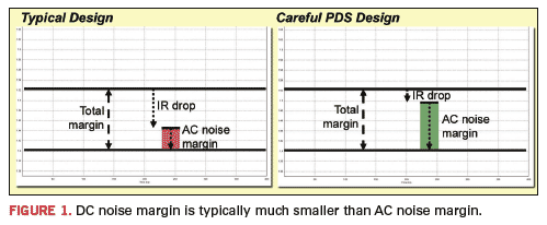
Just as the board design community is becoming familiar with signal integrity, along comes the next hot topic – power integrity. The objective of board-level power integrity (PI) is to assure adequate current is delivered to all mounted devices within a tight voltage margin, as DC power requirements and AC switching activity change dynamically. PI challenges are of growing concern because of several parallel trends. Total power and current requirements are creeping upward, while voltage levels are dropping. With lower voltage comes lower power delivery network (PDN) and signal noise margins. Switching speeds are getting faster and high-speed serial and parallel interconnects are becoming more pervasive.
DC Power Integrity DC PI design flows begin with static power consumption specs, including voltage and current for each power rail, as well as DC noise margins and IR drop constraints. Detailed board-level DC simulation solutions are readily available and run quickly for even large boards. Constraint-driven EDA solutions are more the norm than the exception. DC PI simulations are typically setup early in the design flow and can be quickly performed as incremental validation checks when board designers update the design. Physical prototypes and measurements, based DC PI design flows, are too time-consuming and not flexible enough to meet modern design challenges.
DC noise margins are typically more stringently specified than AC noise margins. It is not atypical to allocate only 20% of the total available PDN noise margin for DC (FIGURE 1). This is possible because their behavior is modeled much more completely than those for AC simulation. This is due to the fact that localized coupling and PDN-global effects, such as resonances, do not exist for DC.
Stackup design is the first task with design controls available for a number of layers and power plane metal thickness. Applying two-ounce copper layers everywhere would help thermal concerns and DC power delivery, but it is unnecessarily expensive and increases overall board thickness and design weight. AC signal routing concerns also drive stackup selection, but only DC simulations are performed to validate choices made at the pre-placement stage in the design flow.
Mounted device placement is the next step, including PDN components such as the voltage regulator module (VRM) and remote sense lines – low current control nets to detect remote voltage levels. Key considerations are high via currents and plane current densities in the region of attachment of the VRM to the PDN. EDA support is available for optimizing sense line placement, which can help recapture significant DC noise margin that otherwise would be wasted.
Vias between planes are an important consideration throughout the entire PDN. They must be placed properly to avoid vias that carry little current, resulting in wasted space and likely current constraint violations. In addition to constraint tables, color-shaded plots are available for both via currents and plane current densities.
AC Power Integrity Typical AC PI design flows are considered in two distinct stages, each of which is reviewed in detail below. The first stage involves frequency domain analysis and measurement techniques to examine frequency-dependent PDN impedance. Capacitors are selected and placed between the power and the ground nets to provide transient switching currents to mounted devices. This task is performed after device placement on the PCB but prior to routing signal traces because routing changes are difficult to make later in the design flow to accommodate additional capacitor placements local to mounted devices. The second design stage is performed after signal routing and involves detailed analysis of both the PDN and the signal nets to examine transient PDN noise. Driver/receiver electrical models couple transient signals with the associated switching current flow in the PDN. Of particular interest for AC PI is the case of many signals switching at the same time, called simultaneous switching noise (SSN).
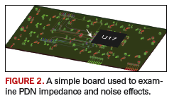
A simple six-layer board design is applied to investigate AC PI effects, as shown in FIGURE 2. The stackup is SGSSPS, where S=signal, G=ground, P=power.
PDN Impedance Low frequency-dependent impedance between power and ground assures low transient noise voltage when currents are pulled through the PDN to drive switching signals. Target impedances are different for each device and sometimes for different pins within the same device. Not all vendors provide specifications for target impedance, but it is easily approximated based on allowable AC noise margin (ΔV) and power rail switching current amplitude (IAC), as Ztarget = ΔV / IAC. For a 1.5-V power rail with +/-5% total noise margin and 80% allocation to AC noise, ΔV = 60mV. A switching current of 5 A implies target impedance for the power rail of 12 mΩ. Since multiple pins exist for each power or ground net, the per-pin impedance would be larger; however, it does not decrease linearly with pin count because switching current does not flow uniformly in all pins. Board-level target impedance is rarely frequency-independent because switching currents have non-uniform frequency spectra. Further, board PDN impedances are dominated by inductance at high frequency and rely on package and silicon for noise filtering and local decoupling capacitors (decaps) to provide on-chip switching currents above 200 MHz to 500 MHz. The simple board of Figure 2 is examined to help understand PDN impedance and the physical effects that cause frequency-dependence. The signal nets are ignored and only the power/ground nets are examined. Frequency domain, board-level AC simulation is performed prior to fabrication, although the same impedance is often measured in the lab for physical prototypes using a vector network analyzer (VNA). PDN impedance is most often characterized for bare boards because precise analysis is difficult due to a lack of accurate models for all devices connected between the power and ground nets of the PDN.
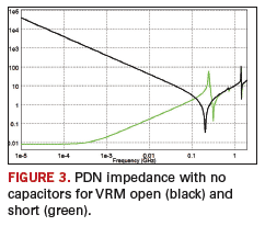
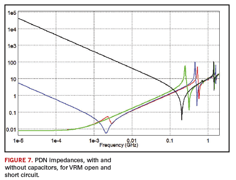
Impedances are characterized looking into the PDN from the location of a mounted device. FIGURE 3 shows the bare board PDN impedance looking into device U17 indicated by a white arrow in Figure 2. An external VRM is connected to the multiple power/ground pins of the card edge connector in the lower/right portion of the board. The black trace is for the VRM open circuit, and the green trace is for the VRM short circuit. The trace is high impedance at low frequency with a slope of -1 on the log-log impedance plot. This represents the capacitance of C=370 pF between the power and ground nets. The green trace, as one expects due to the short circuit at the card edge connector, reflects DC resistance of R=8 mOhm below 250 kHz and loop inductance from the probe to the VRM of L=2.7 nH below 100 MHz.
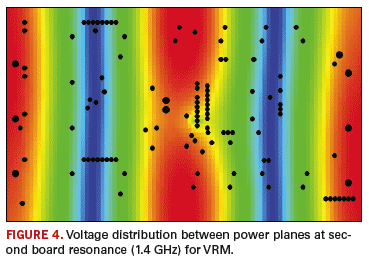
Energy traveling in the board laminate material at 200 MHz has a wavelength of more than 700 mm; therefore, these LC parasitics are lumped circuit effects for this board because the board dimensions are a small fraction of a wavelength. The first dip in the black curve and the first peak in the green curve at 200 MHz are a series LC and a parallel LC resonances. The first plane resonance is where the 100 mm length of the board is a half wavelength, just above 700 MHz. This resonance has a voltage null in the center of the board very near the PDN impedance probe. Therefore, it has little effect on the PDN impedance curves, demonstrating that plane resonances affect various regions of the board in very different manners. The second plane resonance along the length of the board, shown in FIGURE 4, occurs at about 1.4 GHz and has a voltage peak near the probe location. Figure 3 shows the expected large resonance effect at 1.4 GHz. Larger boards have larger-valued L and C parasitics and, therefore, lower frequency lumped resonances. For arbitrarily shaped planes, the resonances are difficult to predict with simple expressions, where the first few resonances were known to be at multiples of a half wavelength along the length of this simple, rectangular board.
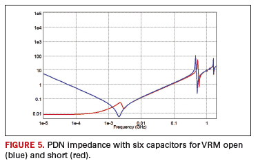
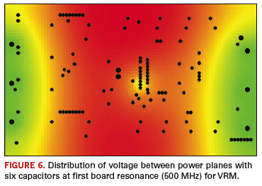
Since plane resonances can dramatically affect PDN impedance, they should be avoided. One way to accomplish this is to add capacitors between power and ground. These capacitors provide switching current and become short circuits at high frequency to eliminate resonances. Six 0.47-nF capacitors are attached to the PDN of the example board – three on each the left and the right side. These are typically called decoupling capacitors (decaps). They add to the lumped C parasitic of the board; therefore, the lumped LC resonances drop to about 200 MHz, as shown in FIGURE 5. At higher frequencies, the capacitors form a low-impedance path between power/ground planes and significantly change plane resonance patterns. Voltage maxima, previously at the left/right edges for the first plane resonance, become voltage minima, with a voltage maximum now near the probe. The loading of the capacitors drops this resonance to about 500 MHz, with a voltage distribution as shown in FIGURE 6.
Above the 2-MHz-lumped LC resonance, the impedance becomes inductive (slope of +1). With the addition of six decaps, the effective inductance is reduced because additional low-impedance current paths now exist at the edges of the board through capacitors. This can be seen in FIGURE 7 by comparing the red and green traces above 2 MHz and below the first plane resonances. If more decaps are placed on the board, the resonances are further changed and the high frequency inductance-dominated PDN impedance is further reduced.
This process of adding decaps, examining resonances and then choosing new decap locations and values can become tedious for designs that require more than a handful of decaps. This process is usually simulation-based and implemented in commonly available EDA solutions. Measurement-based flows are rare because physical prototypes require too much time to manufacture, and it is difficult to measure resonance voltage distributions to know where to locate new decoupling capacitors. The effort involved in crafting a low-impedance profile through analytical decap placement and component selection leads many designers to over-design unnecessarily expensive boards with too many decaps. Design rules are applied, such as use one decap per power pin and apply the largest decap available for a given component size. It is rare this many decaps are required and, as demonstrated in the previous example, using a larger-valued decap leads to a lumped resonance frequency that is potentially too low. There are EDA solutions that can optimize board designs for high-performance (low PDN impedance) and low-cost decap schemes. These solutions are applied at the post-placement/pre-route stage, during post-layout verification or even for post-production enhancements.
PDN Noise Design goal specification and measurement verification of both PDN and signal noise is ultimately a time domain issue for end products. PDN noise is a function of the transient currents pulled by switching circuits to drive signals between logic states. Therefore, PDN noise is dependent on signaling conditions. Lower target impedances should be specified for frequencies with high switching current content. Since signal nets reference the local PDN to define signal voltage, PDN noise results in higher signal noise. If many signals in a region of the board switch at the same time, there can be high switching current flow in the PDN, resulting in high signal noise. In addition, if the signals all switch simultaneously from one logic state to the other, signal net proximity couplings can sum to become larger. This condition is called simultaneous switching noise (SSN) and is of great concern for DDR memory buses and multi-channel, high-speed serial interconnects. SSN is commonly perceived as a signal noise issue, but this simple board example demonstrates it is dominantly a PDN issue.
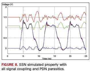
PDN noise is characterized for the same simple board for which PDN impedance was previously examined. The six decaps added are retained because the PDN impedance is lower with them present. The same PDN probe location is applied, only now, transient simulation or an oscilloscope are applied to characterize the PDN in the time domain. IBIS drivers are specified for the 16 single-ended signal nets with signal sources at the mounted device U17 on the top of the board. Eight resistive terminations are applied at each of two separate memory devices on the board. The signals are routed on a combination of the four signal layers, with the bulk of the routing occurring on the bottom microstrip and two middle stripline signal layers. As recommended for SSN simulations or measurements, one signal is tied high, one is tied low and the other 14 signals are switched simultaneously. A 010101… switching pattern does not produce worst-case noise, but it will demonstrate the relevant issues. Voltage probes are placed at the memory device locations for the 14 switched signal nets and at the driver for the two tied high/low signal nets.
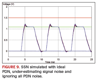
FIGURE 8 shows the board-level simulation results for this SSN case. All parasitic effects of the signal nets and the PDN are considered in the simulation. The PDN (red trace) shows a noise voltage level of nearly 500 mV. The green trace is the signal net tied high and has noise voltage of 400 mV. The blue trace is the tied low signal and has a noise voltage of 150 mV. The 14 switched signal nets experience significant ringing in the high state, as well as significant ringing and skew in the low state. Notice how the PDN noise corresponds closely to the higher-frequency signal noise. The board-level simulation algorithm was manipulated to ignore PDN while retaining all signal net parasitics. FIGURE 9 shows the results results with no PDN noise and the tied high/low signal net noise is zero. Significantly reduced levels of initial overshoot, ringing and skew are observed for the signals.
These simulations clearly demonstrate the dominant contribution of PDN effects to SSN noise. PDN noise is seen to be a significant contributor, due to both plane effects and via/trace/pad parasitics of device mounting structures. The results of Figure 9 are common to a majority of EDA signal integrity (SI) solutions because they assume an ideal PDN and do not simultaneously consider power integrity effects. Application of such SSN simulations yields an unacceptably low prediction of signal noise and completely ignores PDN noise. Coupled SI-PI simulation enables reliable prediction of signal-dependent PDN noise, which in turn can be applied to reliably predict board-level emissions under actual operating conditions – a task not practical for SI or PI simulation alone.
Conclusion Power integrity is all about noise, with margins for both DC and AC noise contributions. In the sense that DC is just another frequency point, the vast majority of post-placement/pre-route PI simulation and measurements are performed in the frequency domain. Stackup design, VRM/component placement and current constraints for vias/planes are key issues. Pre-layout AC PI design challenges relate to crafting a low PDN impedance profile with proper placement and selection of decaps. Decap placement and selection are based on PDN resonance behaviors that are fairly easy to understand, demonstrated here or automated by EDA solutions. Post-layout verification of SI and PI are tightly coupled concerns because both are depend on signaling conditions. PDN effects play the dominant role for SSN, and reliable simulation of SSN cannot occur in their absence. pcd&f
Brad Brim has product marketing responsibility for Sigrity in the area of PCB and package simulation; This email address is being protected from spambots. You need JavaScript enabled to view it..
The proper design of the power distribution network, coupled analysis in the early design phases, can eliminate most power integrity issues.
A number of recent trends – the growing number of different voltages on a design, coupled with increasing power demands from integrated circuits (ICs), as well as the ever-present issues of increasing operating frequency and the need to reduce product cost – have caused power integrity (PI) issues to become more and more of a problem in today’s electronic designs. Since both PI and signal integrity (SI) problems often turn up as data errors, PI issues are frequently misdiagnosed as SI problems. Thus, an understanding of power delivery issues is essential to the success of a PCB design.
The goal in designing a power distribution network (PDN) for a PCB is simple: minimize the impedance between power and ground for your frequency range of interest. Successful execution of that design goal is not quite as simple.
The PDN consists of: a combination of the DC-to-DC converter or voltage regulator module (VRM) supplying voltage to the rail; the decoupling capacitors tied between power and ground; the planes and/or traces carrying power; on-chip decoupling; and the pins and vias connecting all these elements together. The VRM is very effective in providing a low impedance path between power and ground, up to around 1MHz. For the remainder of frequencies, the low impedance between power and ground must be provided by the board and chip capacitances.
The board and chip capacitances combine in parallel but are each limited by their parasitic inductances and resistances. Without parasitics, all the capacitances would combine to make one large capacitance, equating to a lower impedance with increasing frequency. Unfortunately, each capacitance is only effective in a given frequency range, limited by its parasitic inductance. Because the amount of capacitance between planes is typically limited by area and spacing, the plane capacitance does not equate to a low impedance until higher frequencies. As such, each of the board capacitances is only effective for a certain frequency range and must work together to provide a low impedance between power and ground across the entire frequency range. An example plot of impedance versus frequency is shown in FIGURE 1.
A factor limiting the effectiveness of the board capacitances is chip/package inductance. This additional inductance adds to the parasitics of the board capacitances, making them ineffective above about 1 GHz. Above 1 GHz, the on-chip capacitance (not limited by the inductance of the package) provides the low impedance path between power and ground. As such, board decoupling is typically analyzed between about 1 MHz and 1 GHz, and board PDN design is focused at minimizing the impedance between these frequencies.
Maintaining a low PDN impedance introduces a number of benefits. The most direct benefit is minimizing the amount of voltage ripple at the IC supply pins. In fact, the tolerable amount of voltage ripple at the IC supply pins is what determines the maximum allowable PDN impedance. The PDN impedance requirement may be calculated using the following formula: Zpdn = (% ripple * V) / Imax where V is the rail voltage and Imax is the peak current draw of the IC. As such, ICs with higher current draw and lower operating voltages require a lower PDN impedance.
Another benefit of a low PDN impedance is the reduction of noise propagation throughout the board. Power pins, signal pins and vias can introduce noise onto the planes that can propagate around the entire PCB. The presence of low impedance paths between power and ground facilitates better flow of return currents.
At DC, the problem becomes much simpler, but failures can be much more severe. The goal is still to minimize the impedance of the PDN, but at DC, the main concern is providing an adequate amount of metal to distribute up to tens-of-amps of current. With planes being partitioned up to accommodate the growing number of different voltages on a PCB, this can be quite a daunting task.
Analysis of plane shapes within the PDN can be very useful in identifying areas of low voltage. Areas of the board where voltage dips below a certain minimum threshold can lead to IC malfunction, including, but not limited too, signal integrity problems and logic errors.
Of equal concern are areas of high current density on the board. These can be caused by neckdowns due to the partitioning of the plane, but they are also common in dense connector and IC pinfields, where antipads eliminate a great deal of the copper on plane layers. Areas of high current density lead to voltage drop but can also lead to board failure. Analysis of the PDN at DC will also produce this useful current density information. It is also important to monitor current through vias connecting planes together or VRMs to planes. Vias can act as similar neckdowns and areas of high current density, resulting in similar failures.
Through an understanding of proper design of a power distribution network, coupled with analysis early in the design phases, severe issues with power integrity can be avoided. This ultimately results in meeting schedule and budget goals, while designing products that are more reliable and last for many years to come. PCD&F
Patrick Carrier is a technical marketing engineer for Mentor Graphics.
Driven by production adoption, happy days are here at last.
In an era of slower growth and limited investment, wafer-level packages (WLPs) are bucking the trend, with unit volumes expected to top 12.5 billion die this year. What is driving WLP shipments in what for many package types is an otherwise slow year? And what is the impact on major IC package contract assemblers?
As end-users continue to strongly prefer small form factor, low-profile consumer products, small packages such as WLPs meet the requirements. Demand for thin packages and greater functionality in smaller spaces drives the increased adoption of WLPs in mobile phones. Cell phone makers are increasing WLP use. Under the most pessimistic scenario, more than a billion handsets are expected to ship this year. Many Japanese DoCoMo phones contain four to nine WLPs per handset. Shipments are growing as many companies convert leaded packages into WLPs in the search for low-profile packages. In addition, the perception is WLPs are less expensive because they have no substrate or wire bonds. Many companies are designing wireless devices in WLPs, resulting in growth for 300-mm wafers, whereas many early WLPs were fabricated on 200-mm or smaller wafers. However, demand for 200-mm wafers is also increasing.
WLPs are also found in an increased number of consumer products (PDAs, watches, MP3 players, cameras and digital camcorders) and are expected to see greater use in laptops.
Issues and improvements. Wafer-level packaging requires a good material set and process, as well as test and backend processes such as wafer thinning and sawing. This can be challenging with copper low-k wafers at the 65-nm and 40-nm nodes. For this reason, companies are looking at improvements in wafer-thinning technology and use of laser singulation to prevent chipping and cracking.
WLPs, often with underfill, are increasingly able to pass the drop test (one of the most important tests for cell phone makers). New processes to make WLPs more reliable are key to greater adoption. Process improvements include increased dielectric thickness, new materials with improved properties and improved designs. Unfortunately, the wide range of lead-free alloys for WLP solder balls makes it difficult to predict reliability from supplier to supplier.
Traditionally, WLPs have been used for a variety of devices with low pin counts and small die sizes. WLPs are used for power MOSFETs, power management, controllers, ringtones for mobile phones, battery management devices, integrated passives, DC-DC converters and some memory devices. RF components such as Bluetooth and wireless LAN devices, as well as diodes, EMI filters and devices for ESD protection, are packaged in WLPs. Many of today’s cell phones contain CMOS image sensors packaged in WLPs using ShellCase technology (now owned by Tessera). The latest image sensors are being fabricated with TSV technology to reduce the size of the camera module for cell phones.
Fan-out WLPs. With increased interest in using WLPs for larger die with higher pin counts, an increasing number of companies are looking at fan-out WLPs. Casio Micronics’ copper post technology has been used for years in cell phones and consumer products such as watches. Infineon developed a “molded reconfigured wafer” technology for its fan-out WLP solution, called eWLB (Figure 1). The chip backside and edges are covered with a mold compound and array interconnect solder balls attached to the active side of the die. This permits use of a fan-out redistribution. The technology is targeted at medium-to-high-I/O count (<300) devices such as baseband processors and multiband transceivers. Several companies have licensed eWLB and production lines have been installed at ASE and STATS ChipPAC. Infineon, STATS ChipPAC and STMicroelectronics are proposing eWLB as a standard for future-generation products.
Capacity expansion. WLP capacity, especially for 300-mm wafers, is in short supply at several major IC package subcontractors, especially in certain geographies. The transport time and logistics to move wafers from the fab to the WLP processing operation cuts into the tight time-to-market that many semiconductor makers are experiencing. Frequent flyer miles are no substitute for WLP stocks. In response, some subcontract assemblers have placed customers on allocation. The announced capacity additions are a welcome signal for advanced packaging equipment suppliers, as they benefit from investment. Happy days are here again – at least in advanced packaging. PCD&F
E. Jan Vardaman is president of TechSearch International, (techsearchinc.com); This email address is being protected from spambots. You need JavaScript enabled to view it.. Her column appears bimonthly.
Reliability is a balance between force and strength, and when the force is greater than the strength of the copper and dielectric material, the PCB fails.
When exposed to thermal cycle testing, copper cracks that develop at an ever-increasing rate in the barrel of plated through holes (PTHs) represent an accelerated failure mode. This is a failure mode where material change plays a major role in how the circuits fail. The damage may have a delayed onset, but once initiated, tend to accelerate until failure as noted by a 10% increase in resistance is complete. Cracks in the barrel of the PTH advance through the metallization and the electrodeposited copper layers, propagating through copper crystals and traversing the barrel in a straight, horizontal path. The cracks are frequently found to be open upon microscopic review.
The resistance graph, FIGURE 1, demonstrates that at the beginning of the test, there was a degree of stress relieving or annealing until 150 cycles. It appears the annealing reduced the stress on the copper traces and interconnections, resulting in a small reduction in resistance for a number of cycles.
The damage accumulation was more or less linear until the resistance increased to 2%, after which, a non-linear acceleration was observed. There was an exponential accumulation of damage observed until failure at approximately 375 cycles. The damage profile in the resistance graph is typical for an acceleration type failure.
Dynamic mechanical analysis (DMA) is a thermal analysis method that measures a material’s viscoelastic properties. The test induces a mechanical displacement in a sample by flexing and measures the material’s resistance to the displacement and its ability to return to the original condition over a range of temperatures. This method measures the relationship between viscous and elastic characteristics of the material that may change in response to thermal cycles. A material that is elastic deforms in response to a force and returns to its original shape when the forces is removed. A material that deforms in response to a force and does not return to its original shape is said to be plastically deformed. Plastically deformed material around a failing PTH may prevent cracks from closing between thermal excursions. It is likely that the acceleration observed in this failure mode is in part due to the slowly accumulating plastic deformation of the dielectric material in response to thermal cycles.
A microsection of a failing PTH with an accelerating resistance profile frequently exhibits barrel cracks that are open at ambient with a gap between crack edges. Once the crack has initiated, damage accumulation begins to accelerate in response to the dielectric material losing elasticity and being plastically deformed. The slowly accumulating plastic deformation of the material, in response to thermal excursions, causes the copper cracks to open and become larger, expanding a little more with each thermal cycle.
Hysteresis is a condition where a system resists returning to the predicted or original state when a force is applied or removed. There is a physical hysteresis that is reflected in the deformation of the material preventing cracks from closing between thermal excursions. Developing cracks are expressed as a hysteresis in the resistance graph at ambient and at the maximum test temperature.
Conclusion Reliability is a balance between force and strength. When the applied force is greater than the strength of the copper and dielectric material, the PCB fails. During thermal excursions, the PTH is under tension from z-axis expansion and, at the same time, an inward compression in the middle of the PTH due to x- and y-axis expansion. Once initiated, copper cracks develop rapidly to produce early failures. This accelerating failure mode is the result of the force, induced by thermal expansion of the material being greater than the strength of the copper interconnections and the dielectric material combined. At the same time, the material loses elasticity and undergoes plastic deformation. PCD&F
Paul Reid is program coordinator at PWB Interconnect Solutions Inc.; This email address is being protected from spambots. You need JavaScript enabled to view it..


 “All of us learn to write in the second grade. Most of us go on to bigger and better things.” – Bobby Knight