VNA is a powerful tool for determining DUT response in frequency domain, but accuracy is influenced by external factors.
The vector network analyzer (VNA) is an instrument suitable for measuring the response of a device under test (DUT) versus frequency.
1 VNA transmits a sweep of sine waves to DUT.
2 It then receives and analyzes reflections to ascertain the reflected signal magnitude, phase shifts, S-parameter models, etc. VNA is a versatile laboratory apparatus capable of measuring numerous device properties including skin effect losses, inductance, capacitance, DUT characteristic impedance, coupling coefficients and variations in dielectric constant.
Some of the fundamental concepts and techniques related to VNA characterization of PCB interconnects will be covered in this column.
VNA is a powerful device for determining the DUT response in frequency domain; however, the measurement accuracy is strongly influenced by factors external to VNA.
3 For instance, the interconnect cables and adapters employed in the measurement setup can cause deviations in signal magnitude and phase, which can obscure the actual response of DUT. In order to minimize such measurement errors, it is necessary to perform a pre-measurement step called calibration.
Two notable calibration approaches consist of the short-open-load-thru (SOLT) and the thru-reflect line (TRL) techniques. The latter is a more advanced method which allows a wider frequency range and higher accuracy.
4The calibration involves vector error correction in which error terms are first characterized utilizing known standards and then eliminated from actual measurements.
5The standard devices entailed for calibration are obtainable in suitable calibration kits
3 with various connector types (such as SMA or SMP). Each calibration kit usually contains impedance-matched load, open circuit, short standard and adapters (for male and female connectors).
It is advantageous to use a torque wrench for tightening coaxial connectors, in order to achieve repeatability and to prolong connector life. Some torque wrench designs encompass a break-over feature (when preset torque is reached) which prevents over-torquing of a coupled junction.
6VNA has the capability of displaying scattering matrix (S-parameters) as a function of frequency on a Smith chart or as magnitude and phase (real and imaginary) format.
The Smith chart represents a polar graph of the reflection coefficient with grid lines displaying values of normalized impedance.
7One effective method for evaluating the quality/accuracy of a calibration involves attaching a standard open, matched load or short (same standard devices employed during calibration phase) to a VNA port and then viewing the associated return loss via the Smith chart display format.
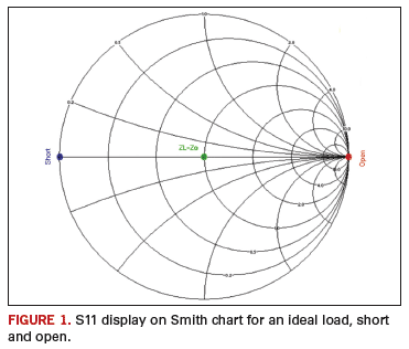
Ideally, on a Smith chart, the S11 response from a matched load, short and open device connected directly to the front connector of VNA should be a dot at the center, a dot at the left side and a dot at the right side of the chart, respectively. This is illustrated by
FIGURE 1.

Most short or open standard devices (belonging to VNA calibration kits) include an offset (for instance, a small built- in delay), the effect of which is not evident at low frequencies. However, at higher frequencies, the delay effect becomes observable. Subsequently, for a valid calibration, the return loss of a standard load will be a dot at the center on a Smith chart, but an open will produce a small arc starting on the right side of the chart and extending into the lower part of the chart (for example, slightly capacitive effect).
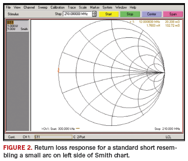
The S11 response of a short appears as a small arc starting at the left end of the chart and extending into the upper part of the chart. This is depicted by
FIGURE 2.

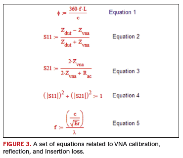
A relationship for calculating such phase shift (arc) caused by an electrical offset is offered by
Equation 1 in
FIGURE 3, where:

Φ = amount of phase shift (in degrees)
f = frequency (Hz)
L = electrical length of the offset
c= speed of light in vacuum
Speed of light appears as a factor in many engineering computations, and it is beneficial to be familiar with value of c in various units. For instance, in the following equation:
c = 3E8 m/sec = 3E10 cm/sec = 30 cm/ns = 1.118E10 in/sec = 0.0118 in/ps = 11.8 in/ns
The reciprocal of c is signal propagation delay in vacuum: (1/c) = 1.02 ns/ft.
This is approximately 50% of the commonly used value (2 ns/ft) for signal propagation delay on a FR-4-based PCB. This implies that signal speed in PCB traces is usually about one-half of free space velocity.
A set of VNA measurements, to be later discussed, were performed on several PCB traces employing an Agilent N5230A (300 KHz to 20 GHz) PNA-L network analyzer. This apparatus can be calibrated manually using a mechanical calibration kit or automatically via an electronic calibration (ECal) module.
One useful feature of the network analyzer is that a calibration state can be saved into memory and later recalled. This can significantly enhance measurement efficiency by eliminating the need for another calibration. However, to minimize measurement inaccuracies when recalling a calibration state, the same cabling and torquing, as in the original calibration, should be applied. Furthermore, voltage drifts caused by temperature variations need to be taken into consideration.
The main output of VNA consists of scattering matrix elements (S-parameters), which are ratios of reflected or transmitted voltages to the incident signal voltage. S-parameters can be applied as behavioral models,
8 and they are extensively utilized in high-speed digital system design for simulation and analyses of passive interconnects.
For a two-port measurement, the resulting S-parameter matrix elements include S11, S21, S22 and S12.
The return loss S11 is a ratio of reflected to incident voltage (for example, S11 = Vref/Vinc). The insertion loss S21 is a ratio of transmitted to incident voltage (for instance, S21 = Vtrans/Vinc).
There are numerous equations governing S-parameters, some of which are listed in Figure 3.
Equation 2 illustrates how S11 relates to DUT impedance (Zdut) and impedance of VNA (Zvna ~ 50 Ohm typically.)
Equation 3 shows how S21 data can be utilized to extract AC resistance of a PCB transmission line.
1 This formula is applicable when VNA impedance is close to DUT impedance, within a frequency range for which trace conductor losses are much greater than dielectric losses.
Equation 4 holds true for a symmetrical system (such as PCB trace) when S11 = S22 and S21 = S12. Furthermore, the system should be lossless (or low loss) at frequencies for which skin effect resistance is low.
1 When a network satisfies these conditions, then extraction of DUT parameters can be significantly simplified.
Another useful relationship is
Equation 5. It allows determining locations of resonance nulls and peaks, which occur on S11 (or S22) and for analyzing the shape of S-parameters.10 Here, c/√Er is signal velocity in medium of permittivity Er, and λ is the wavelength corresponding to signal frequency f.
PCD&FDr. Abe (Abbas) Riazi is a senior staff scientist - hardware development with Broadcom;
This email address is being protected from spambots. You need JavaScript enabled to view it..
ACKNOWLEDGEMENTS
My gratitude to Abbas Amirichimeh, Mohammad Tabatabai, Patrick Zilaro, Mohammad Ali and Sam Karikalan of Broadcom Corporation; and Wenlei Lian of Agilent Technologies.
REFERENCES
1. Stephen H. Hall, Garrett W. Hall, and James A. McCall, “High-Speed Digital System Design A Handbook of Interconnect Theory and Design Practices,” John Wiley & Sons, Inc. 2000, p. 85, pp. 303-317.
2. Roy G. Leventhal and Lynne Green, “Semiconductor Modeling For Simulating Signal, Power, and Electromagnetic Integrity,” Springer 2006, pp. 126 - 130, p. 484.
3. “User’s Guide Agilent Technologies 8719ET/20ET/22ET, 8719ES/20ES/22ES Network Analyzers,” Agilent Technologies, 2002, Chapter 6.
4. Tom Granberg, “Digital Techniques for High-Speed Design,” Prentice Hall, 2004, pp. 540-547.
5. Michael Hiebel, “Vector Network Analyzer (VNA) Calibration: The Basics,” White Paper, 2008 Rohde & Schwarz USA.
6. “MTBN (Break-Over Wrench) Operating Instructions, Rev. 1.0,” mountz the torque tool specialists.
7. “On-Wafer Vector Network Analyzer Calibration and Measurements,” Application Note, Cascade Microtech.
8. Timothy Coyle, “S-Parameters for Digital Designers,”
Printed Circuit Design & Fab, May 2009.
9. Eric Bogatin, ‘Signal Integrity - Simplified”, Prentice Hall, 2004, pgs. 34-36.
10. Greg Edlund, “Timing Analysis and Simulation for Signal Integrity Engineers“, Prentice Hall, 2008, Pgs, 97-100.


