How to increase overall coverage while decreasing the number of physical test points that need to be added to a design.
Today's component densities preclude the incorporation of sufficient test points on the board that would allow for adequate electrical test capability. The Institute of Electrical and Electronics Engineers (IEEE) published the 1149 specification, pertaining to boundary scan as a method to address the issues of reduced test-point access.
Typically, high-pin-count, field-programmable gate array (FPGA) and application specific integrated circuit (ASIC) components have boundary-scan capabilities incorporated into them, while smaller devices have versions available that may or may not support boundary scan. If you decide to implement significant test coverage through boundary scan, look for devices that address the functional requirements of the design, as well as support the boundary-scan standard.
Although boundary-scan components can be used to test non-boundary-scan components, better results are achieved with boundary-scan cluster testing. Increased use of these components will improve the level of automatic fault diagnostics reported during the testing.
Trying to improve testability coverage once a board is completed often results in a suboptimal test solution. Incorporating some simple Design for Test (DfT) techniques as part of the PCB design process can significantly improve the overall testability of the board, while adding little or no overhead to the PCB.
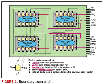
Boundary-scan support can provide a wealth of opportunities for increasing testability coverage, provided that it is implemented properly in the design. A critical element that must be configured correctly is the test access port (TAP). The preferred method is to have all boundary-scan parts correctly chained together with an edge connector to the first test date input (TDI), a test date output (TDO) to subsequent TDI pins and ultimately, a TDO pin that also goes to an edge connector. Then the test mode select (TMS), test clock (TCK) and the optional test reset (TRST) pins are connected together in parallel, also available through the same edge connector. This is illustrated in
FIGURE 1.

One of the advantages in using FPGA and ASIC boundary components is that they typically have bidirectional, boundary-scan cells behind their pins. This means they can be used to both drive conditions onto a net and to monitor conditions on a net. It is this drive/sense capability that is performed by an in-circuit tester when it needs to test the component pin attached to a specific net. Therefore, a boundary-scan cell that is already attached to a net can be used instead of an external driver/sensor from a tester, which, in turn, requires a test point to connect electrically to the PCB. This capability is a boundary-scan cell’s main use when providing test access without the addition of physical test points.
However, most designs use a number of FPGA or ASIC components with unused pins that have the boundary-scan circuitry within. Once these are routed to non-boundary scan nets, the test capability is then available through the scan chain. Not all non-boundary scan nets may be accessible through unused scan pins, but implementing this technique can reduce the requirements for physical test points.
It is important to collaborate with the test engineering department so that the correct priority is placed on nets requiring physical and virtual access through boundary scan. Most designs require that boundary scan be complemented with another test technology, such as in-circuit test or flying probe.
Boundary scan has the ability to be a significant technology to address the issues of reduced access. However, to fully utilize the capability of this technology, it requires the collaboration of both design and test engineering to develop and to implement an optimized test strategy that is capable of delivering on the necessary production volume and quality goals.
PCD&FMark Laing is a product marketing manager, Systems Design Division, Mentor Graphics Corporation;
This email address is being protected from spambots. You need JavaScript enabled to view it..


