Working together, PCB designers and fabricators can explore manufacturing techniques that optimize designs, reduce routing layers and minimize PCB costs.
Fine-pitch BGAs are making PCB designers think twice about implementing traditional fan-out patterns. Now, the burden is on the designer to carefully study a board design and to devise certain fan-out strategies that don’t adversely affect fabrication requirements. There are several major considerations involved in selecting the correct fan-out/routing strategy, including ball pitch, land diameter, number of I/O pins, via types, trace width and spacing, pad size and the number of layers required to escape the BGA.
Here, two different design scenarios are explained. Both are centered on a 0.4-mm BGA lead pitch. The first one is a microBGA on an 18-layer board that includes eight signal routing layers. Normally, for BGA routing, a greater number of layers is required.
However, in this example, the number of layers is not an issue due to the fewer number of BGA pins involved. However, the main problem is the BGA’s narrow pitch of 0.4 mm, and the problem that routing is not allowed on the top layer, except for fan-outs. The goal here is to fan-out the BGA without adversely affecting board fabrication.
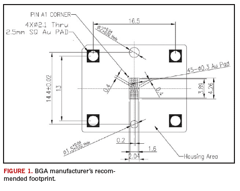
FIGURE 1 shows the footprint from the BGA device’s manufacturer. As shown, the recommended pad size is 0.3 mm (12 mils), and pin pitch is 0.4 mm (16 mils). It’s not possible to have the traditional dog-bone fan-out pattern due to the extremely small space between the pads. Even a small-sized via cannot be used for a dog-bone fan-out strategy; here, a small-sized via means a 6-mil drilled hole with a 10-mil pad. Another important mechanical limitation is the board thickness, which is 93 mils.

In this case, the easiest solution is using microvia-in-pad; however, the microvia size cannot be more then 3 mils. This is because the 93-mils board thickness is a limiting factor. Another option is blind and buried via technology. These options will limit manufacturing choices and increase costs.
It is advantageous for the designer to discuss manufacturing capabilities with the PCB fabricator during the design process. Many PCB fabricators have a 6-mil minimum drill size for a 93-mil thick board and may limit minimum trace width to 4 mils. Designing smaller holes and finer trace widths will reduce the number of fabricators capable of producing the PCB to a handful of high-end board manufacturers, likely resulting in a higher-priced board.
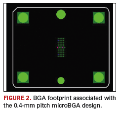
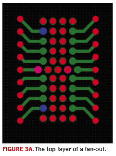
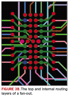
FIGURE 2 shows the BGA footprint associated with this first case study. The fan-out method devised here avoids using a high-end technique and doesn’t jeopardize signal integrity. BGA pins are divided into two sections, internal and external pins. Via-in-pad is used for the internal section, while external pins are fanned out at a 0.5-mm grid.
FIGURE 3a shows the top layer;
FIGURE 3b shows top and internal routing layers.


Since BGA pad size is 0.3 mm (12 mils) and pitch is 0.4 mm (16 mils), a 6 mil/10 mil via (hole/annular ring size) is used in the pads. The same via is used for external extended fan-out. For the internal section, clearance between vias is 6 mils, which is routinely standard and doesn’t pose a problem at fabrication. For the external section, spacing between vias is 10 mils. This spacing is used to run a 3-mil trace with a 3.34-mil distance from the vias. This particular strategy allows all signals from a 0.4-mm pitch BGA to be successfully fanned-out without complying with any special fabrication requirements.
Dealing with RF and Differential Signals
While the main issue was the narrow 0.4-mm pitch in the design example above, this second design case poses another major one. The goal here is to maintain the critical signal integrity of RF and differential pair signals. That’s in addition to the concerns dealing with performing a successful fan-out for a 121-pin, 0.4-mm pitch BGA and sidestepping major board fabrication issues.
The BGA is mounted on an 8-layer board with six routing layers, including top and bottom. Signals coming out of the BGA consist of digital data buses, high-speed differential and low amplitude RF. Of these, the RF signals are the most critical, with signal integrity being of prime concern.
While doing the layout of low-amplitude and high-speed RF signals, impedance matching is of the highest concern. These RF signals are being used to communicate with the µP to the wireless USB.
These signals need to be routed on the top layer and come out of the outside perimeter of the BGA. The differential signals also need special attention. They must be fanned out from the center of the BGA, the reason is due to the design constraint of the chip.
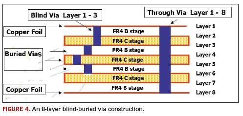
Initially, the BGA was routed with the standard fan-out pattern and stackup for a 0.4-mm BGA using blind and buried vias. The outer perimeter was routed on top; the inner perimeters had the following set of vias, shown in
FIGURE 4.

The suggested stackup of the multilayer board included a through via from Layer 1 to Layer 8, a blind via from Layer 1 to Layer 3 and buried vias from Layer 3 to Layer 4, Layer 4 to Layer 5 and Layer 5 to Layer 6.
After a consulting session with the fabrication house, issues with this via stack became apparent. The conclusion reached was that this type of stackup requires numerous lamination cycles, both time consuming and costly, and the expected yield would be less than 30%.
Also, due to the use of the fan-out pattern for the blind and buried vias, the signal integrity of the differential signals would be compromised, since they are coming from the BGA’s center.
Another consultation with the fabrication house confirmed it had the expertise and capabilities for 0.4-mm pitch packages, so the solution was at hand. This fab house could easily do 4-mil mechanically drilled through-holes in a 0.062-inch thick board. As it turned out, this particular design is based on a 0.062-inch board. The 4-mil drilled hole size could accommodate a 7.5-mil pad with 12-mil anti-pad. This allowed a 3-mil trace to go through the center of two such vias placed on a 0.4-mm grid. The vias were silver filled, and a gold plated final finish provided a flat surface for the BGA.
This is a simple, yet effective solution. The main concern was to fan-out the outer perimeters of the BGA with layers that were deepest in the center of the stackup. As we go to the center of the BGA, we would go to the outer layers. The reason for this is some fabricators may only be able to drill a 4-mil hole in 0.032-inch laminate. In this case, they treat this type of project as two boards and use two lamination cycles. Note that this type of fan-out is done to avoid drill wander, which is detrimental in fine pitch products.
By using the 4-mil vias on the BGA pad, this particular design achieves 100% accessibility to all BGA pins without compromising the signal integrity to any of the critical signals. It also keeps the board cost to a more acceptable range.
A Case for Through Vias
It is quite possible to use through vias with via-in-pad designs involving 0.4-mm pitch BGAs. The trade-off, however, is that it requires specialized manufacturing techniques.
From a design perspective, it involves treating a 0.4-mm pitch BGA like a 0.65-mm one and putting the vias exactly in the center of each BGA pad. The vias are silver filled in one of the last fabrication process stages to provide a flat surface. Via size is a 4-mil drilled hole with a 7.5-mil pad and 12.7-mil anti-pad. The only limiting factor in this scenario is the board’s maximum thickness. With a 4-mil drilled hole, most fabricators can only manufacture a maximum 0.062-inch thick board. In this case, an 8-layer board is used.
As a final note, PCB designers continue to encounter challenges associated with routing high-speed signals from a BGA package. Most of the designs using BGA packages have some high-speed signals coming out of the device. Examples of these are SerDes devices and DDR controllers. In most cases, specialized routing techniques, completely out of the norm, must be used. Design experience dictates that it is best that all critical signals, whether they are differentials or single ended, are best laid out (as far as signal integrity goes) if they are on the outside periphery of the BGA. There are several reasons for this:
Use of external layers to route these pins reduces the number of layers required. Routing high-speed traces helps in the propagation time because of the difference of the effective dielectric constant (Dk) between internal and external layers. High-speed signals do not have to pass through vias in the BGA, which helps in a clean signal.
There is no need for the high-speed traces to neck down inside the BGA package to reach their respective pins. Necking down the traces inside the BGA will cause impedance mismatches, which may be detrimental to signals in the GHz range.
Conclusion
As BGA packages continue to handle more I/Os with minimum increase in size, signal escape routing can be quite difficult. The number of PCB layers required to escape all the pins depends on several factors. Some of these factors, like the ball pitch and land size, are device specific and need to be factored prior to starting board layout. The others have to be figured out by the designer. Board designers will always be pushed toward using the minimum number of routing layers to reduce cost, especially when using a strip line structure. Hence, successful and effective routing will always be a challenge for the PCB designer.
PCD&FIshtiaq Safdar is a PCB layout engineer for NexLogic Technologies. Syed Wasif Ali is a C.I.D+ PCB layout engineer for NexLogic Technologies. You can contact them at
This email address is being protected from spambots. You need JavaScript enabled to view it..


