Isotropic routing systems can help reduce the total wire length by 25% to 40%, while reducing the number of vias.
Sometimes, new things have a hard time breaking through, even when they are long forgotten old things. More than 40 years have passed since the publication of the “wave” algorithm - i.e., the Lee algorithm - for solving maze routing problems, as well as the appearance of the earliest grid autorouters. Before the introduction of automated design systems, printed circuit topology was designed manually. It was natural that nobody drew polylines instead of straight lines; moreover, the angles of wires were usually rounded. The look of the first printed circuit boards (PCBs) designed by automated systems caused discontent, perplexity and rejection, but as time passed,
CAD systems became more sophisticated and efficient. Gradually, designers grew accustomed to the shape of the wires and accepted the solution, especially since automation had considerably increased their productivity.
After 40 years, a whole generation of specialists changed, and now there a very few people left who can still remember manual design. These days, the non-orthogonal layout with rounded wires are perceived by many as something absurd, irregular and unconventional. One of the most frequently used arguments is, “Orthogonal topology looks good, and arbitrary-angle topology does not.”
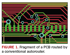
FIGURE 1 shows a fragment of a PCB routed by one of the popular autorouters. One can see numerous bent wires that are easy to explain but not to justify.
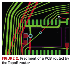
FIGURE 2 shows a fragment of a board routed by the topological router.
1 In regards to aesthetics, tastes differ, so let’s consider the technical side.


Routing is searching for a compromise solution for laying out multiple routes, while meeting a number of conflicting criteria (total wires length, number of vias) and observing different design and technological constraints, which are primarily metrical. Usually, due to the complexity of the task, no attempt is made to achieve a topology that would be optimal in any sense. The stated purpose is to achieve the maximum rate of complete routes.
In most printed circuit
CAD systems, the task of routing interconnections is defined as an iterative search for paths between pairs of points in a maze formed by contact pads, keepouts and previously routed wires. The laid out path is locked and becomes part of the maze.
As a result of limited throughput capacity of the printed circuit areas, the routes are often excessively long; therefore, the number of vias increases. Having to go around the stationary component increases the length of the route and creates obstacles for laying out other routes.
All other tasks (minimization of the total wire length and the number of vias, moving the wires apart locally to reduce spurious coupling, etc.) are usually done after the main result is achieved. These improvements are made to the single topology variant that has been obtained. Of course, refinement possibilities presented by such localized procedures are quite modest. In most cases, the primary criterion for assessing the routing quality is whether the circuit works at all.
Meanwhile, the important topology quality indicators that are overlooked include workability and reliability, which depend in part on: the number of bottlenecks with minimal clearance and their length, the length of parallel paths on each layer, and the conductor overlap area on adjacent layers.
PCB Space Utilization
Popular printed circuit topology design systems route the wires along paths that are vertical, horizontal or slanted at a 45-degree angle.
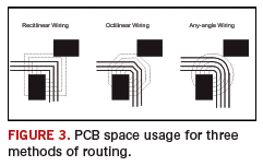
FIGURE 3 demonstrates the advantages of any-angle routing. One can see that only the rightmost variant allows laying out four routes instead of three in the gap between the rectangular regions because PCB space is used more efficiently.
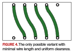
 FIGURE 4
 shows a sample case where the required clearance can be provided only by smoothed wires. The wires pass from one circular arc to another; the required clearance is maintained along the whole length. Any diversion from the circular arc path will lead to a clearance violation. Therefore, any-angle routing with smoothed wires provides more efficient PCB space utilization. Remember, the area of a circle is always less than the area of a circumscribed polygon.

Smooth, Non-Bent Wires
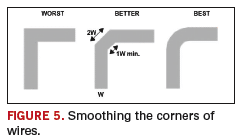
To a large extent, the conducting pattern defines the workability and the manufacturing reliability of PCBs, so when routing wires, one should avoid sharp corners. Inside a sharp corner, a kind of pocket is formed with poorly etched areas, where solder buildups and spikes are formed during soldering. Due to a slight compression stress in galvanic deposits induced by soldering temperature, a sharp corner may peel off the base. If a wire has high electric potential, the corner apex gains high electric-field gradient; contaminations are accumulated at this point due to electrostatic deposition of dust. This creates an electric breakdown hazard.
2At the place where a conductor makes a 90-degree turn, signal bouncing may occur. This is mainly due to the change of wire width. At the corner, the route width is increased 1.414 times, which results in transfer line parameter discrepancy.
3Predominant Layer Routing Directions
One should keep in mind that when the PCB is heated during heat treatment, thermal reflow, drying, soldering, etc., the balance of patterns on the two sides of the board substantially affects its deformation ratio due to the difference in mechanical stress. The widely used rule of opposite sides’ pattern orthogonality leads to twisting of a PCB.
2It should be noted that the cause of the twisting is not pattern orthogonality itself, but the global directional uniformity of the conductors on the layer. In the topology created by an isotropic router, the wires in adjacent layers are roughly orthogonal, but in different areas of the board, the directions vary (
FIGURE 5). That is why layer anisotropy is not a global effect.

Electromagnetic Interference Level
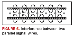
Wires located opposite one another on adjacent layers form a long film capacitor. If two conductors are close to each other, then capacitive and inductive coupling occurs between them, as illustrated in
FIGURE 6.

It is necessary to remember, that every new via, i.e. interlayer connection, adds spurious inductance. For example, if the opening has a diameter of 0.4 mm and is 1.5 mm high, then its inductance is 1.1 nH.
3An isotropic
CAD system almost never creates long wire segments laid out parallel to each other in adjacent layers. The option to specify the minimal and nominal clearance between wires significantly reduces the number and the length of bottlenecks on a single layer. The number of vias in the topology produced by an isotropic routing system is usually many times less compared to the topology created with any other system.
All aforementioned factors, along with reduction of total wire length and absence of predominant routing directions, help decrease the electromagnetic interference level.
When looking at wires going smoothly around obstacles, developers often note that a straight wire has much less inductance than an arced one, making the conclusion that the topology created with an isotropic
CAD system has greater overall inductance. In reality, most
CAD systems perform routing with a predominant direction on each layer; therefore, wire direction rarely changes on a single layer.
In order to estimate the wire inductance, it is not the individual layer topology that should be considered but the combined topology. This will clearly show not only wire bending, but even loops. Loop inductance depends on the loop area, and it does not matter whether it is rectangular or circular. The surface area of a wire laid out by an isotropic routing system is usually considerably less than in other
CAD systems. It should be noted that rounding of prominent corners reduces the area of a convex geometric shape.
Complexity and Cost of Manufacturing
One of the factors affecting the PCB manufacturing cost is the number of vias per square decimeter. On average, the estimated cost of vias is one dollar per additional 300 (exceeding 250) vias per square decimeter. The durability of a hard-alloy drill is about 1000 hits before requiring resharpening. The average price of one drill from 0.3 mm to 3.0 mm in diameter is about two dollars.
An excessive number of holes increase manufacturing cost and drilling time; every 1000 holes take an extra 2.5 minutes to 3 minutes of drilling per board stack. This results in considerable material and time expenses for large-scale and mass production.
During development of multilayer PCBs, one of the aims to achieve is minimizing the number of layers because each extra layer significantly increases the cost. For boards employed in high-performance and high-frequency systems, increasing the number of signal layers requires twice as many layers to maintain the transmission line characteristics and the addition of signal layers often adds additionalground and power layers to provide shielding in such devices.
2Conclusion
In boards with BGA components, the number of layers often depends mainly on the number of pad rows of such components and on established technological constraints, such as the minimum wire width and minimum clearance. In a number of
CAD systems, BGA component internal space routing is performed according to a template because the main purpose is to avoid blocking pads and to lead all routes to the component’s outer edges. But prescribing the mandatory routing directions results in layout deterioration and does not consider the fact that if a microchip has equipotential and non-connected pads, then in some cases, the number of layers needed to provide connections can be reduced.
Compared to other systems, isotropic routing systems can help reduce the total wire length by 25% to 40%, while reducing the number of vias, freeing up more board space. It is possible to either increase wire clearance and contact pad size or to reduce the board size or the number of layers.
PCD&FReferences
1. S. Yu. Luzin, Yu. T. Lyachek, O. B. Polubasov. Printed circuit design automation. TopoR topological router. St. Petersburg, SPbGETU “LETI”, 2005, p. 163.
2. A. Medvedev. Printed circuit boards. Design and materials. Moscow, Tecnosphera. 2005, p. 302.
3. Bruce Carter. Circuit Board Layout Tchniques. http://focus.ti.com.cn/cn/lit/ml/sloa089/sloa089.pdf .
Sergey Luzin is a head of Eremex St-Petersburg Department; luzin@eremex@com. Oleg Polubasov is a head of Algorithmic Department;
This email address is being protected from spambots. You need JavaScript enabled to view it..


