Interviews with the NPI Award winners provide a fascinating view of the investment that goes into taking a new product from concept to production.
There is nothing more important to the growth of an industry than innovation. New product introductions have provided the foundation for most of the technology advancements seen in the electronics industry over the past 50 years.
In November, the IEEE Spectrum published a list of 100 companies ranked by R&D expenditure in 2007. It is not surprising that many of the top 50 were in the electronics industry. Nokia claimed the top electronics industry spot, spending a whopping $8.823 billion in 2007, 10.2% of sales. Samsung came in second, spending $6.162 billion, only 6% of sales, and Intel came in third, spending $5.755 billion, that was 15% of sales.
Another recent studies, however, suggested that the electronics industry as a whole was not investing heavily enough in R&D to keep the invention engine running. A recent report published by Industry Week magazine, “R&D Spending: By the Numbers,” indicated that the electronics industry R&D spend in 2007 was, on average, only 7% of sales, about half that of the software/Internet industry. The industry reporting the lowest R&D spending (1% of sales) was the chemical industry.
It takes a substantial investment to move a product from idea to practice. Some new products provide evolutionary improvements to the existing process by increasing yields, lowering costs or reducing process time. Other technologies are more revolutionary in nature, not only changing the specific process that is being replaced, but also rippling through the entire design and manufacturing stream.
Evolutionary new products are readily adapted into the existing manufacturing scenarios, while revolutionary changes often require time to develop the up- and downstream technologies needed to facilitate wide spread adaptation. Microvias would be a good example of a revolutionary technology. A number of processes were available for building HDI/microvia products in the 1990s, but today, nearly 20 years later, design teams are still learning how best to place and route microvias to maximize the benefits of the higher-density circuits afforded through the implementation of microvias versus traditional through-vias.
In 2009, Printed Circuit Design & Fab joined Circuits Assembly in recognizing the efforts put forth by suppliers in our industry to research, invent and introduce new products. Companies that are actively involved in product introductions are making investments that benefits the industry everyday, and we applaud those companies who have contributed to the advancement of the art.
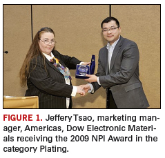
This year, 10 companies were recognized in the areas of PCB design and fabrication. Over the next few months, through a series of interviews, we will provide some additional insight into the companies and people who have been instrumental in these new developments. We will begin with one of our fabrication process winners, Dow Electronic Materials (formerly Rohm and Haas Electronic Materials). We spoke with Jeffery Tsao, marketing manager, Americas, Interconnect Technology at Dow Electronic Materials after he received the award (
FIGURE 1).

NPI Award Winner, Dow Electronic Materials
Category: Plating
Product: Microfill EVF
PCD&F: Who are the key researchers involved in the product’s research and development effort?
Jeffery Tsao: Mark Lefebvre is a Research Manager at the Dow Advanced Materials division of the Dow Chemical Company in Marlborough, Massachusetts. Mr. Lefebvre is responsible for the global development of electroplating processes for Interconnect Technologies, including MicroFill EVF. He received his Bachelor of Science degree in Chemical Engineering from the University of Massachusetts Lowell. Mr. Lefebvre has been involved in Printed Circuit Board technology for over 23 years, 17 of those with Shipley, Rohm and Haas and now Dow Chemical. He has previously published and presented several papers on PCB topics and holds several patents in this field.
Elie Najjar is a Sr. Engineer at the Dow Advanced Materials division in Marlborough. Mr. Najjar was the Project Leader, responsible for the development of MicroFill EVF. He has over 10 years of product development experience in electronic materials imaging and metallization technologies. Mr. Najjar received his Bachelor of Science degree in Chemical Engineering from Northeastern University, Boston, MA.
Leon Barstad is an Engineer at the Dow Advanced Materials division. Mr. Barstad was a project team member for MicroFill EVF Copper Via Fill, and he has over 28 years experience in the Printed Circuit Board industry and holds several patents in metallization technology.
Luis Gomez is a Senior Scientist at the Dow Advanced Materials division in Marlborough. Mr. Gomez was a project team member for MicroFill EVF Copper Via Fill, and he has 20 years experience in the PCB industry. Mr. Gomez received his Bachelor of Science degree in Chemistry from Lehman College.
PCD&F: Why is this product important to the PCB industry?
Jeffrey Tsao: Driven by the need for increased speed and portability of consumer electronics, the interconnect pitch on semiconductors, packages and the corresponding High Density Interconnect (HDI) substrates continue to shrink. Thinner and more uniform surface copper deposits have to be produced, increasingly difficult microvia geometries must be filled and through-hole throwing power delivered, while maintaining plating rates capable of delivering production throughputs. These demands often exceed the capability of current commercial copper electroplating.
MicroFill EVF Copper Via Fill provides enhanced via filling performance, with simultaneous through-hole plating, at a low surface thickness that is unattainable by previous generation systems. Formulated to operate over a broad range of operating conditions, MicroFill EVF Copper Via Fill can be tuned for both HDI and IC Substrate applications, offering end users unmatched production flexibility.
PCD&F: What types of benefits will users see?
Jeffrey Tsao: The process can provide the following:
- Compatibility with both panel and pattern plating processing
- Simultaneous via fill and through hole plating
- Flat pad and trace profile for reliable interconnections and build-up construction
- Tunable to specific customer requirements
- Insoluble anode DC process for consistent operation, eliminating idle time effects
- EVF components can be monitored by existing CVS equipment
- Proven system for HDI and IC Substrate high volume manufacturing
NPI Award Winner, Sigrity Inc.
Category: System Modeling/Verification Tool
Product: Channel Designer
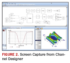
Back in January, Sigrity announced the release of Channel Designer, positioning the product as an analysis solution that offered the flexibility and accuracy needed to predict bit error rates and to ensure reliable operation at speeds at and above 10 gigahertz. We talked with Leslie Landers, VP of sales and marketing for Sigrity after Channel Designer (
FIGURE 2) won the 2009 NPI Award in the System Modeling/Verification Tool category.
 PCD&F:
 How did the idea for the product come about?
Leslie Landers: We’ve become aware of the growing importance of high-speed serial links in system designs. This channel design approach has become the primary method of chip-to-chip interconnect. From the beginning, Sigrity customers used our analysis tools to characterize individual channel components such as IC packages and printed circuit boards. While this is beneficial, we realized the potential for a more streamlined approach to looking at critical channel-wide issues, such as bit error rate prediction and cross talk mitigation.
PCD&F: How long was the product in development and beta site testing?
Leslie Landers: Channel Designer was in development for more than a year, and the beta period was three months.
PCD&F: Who are the key researchers involved in the product’s research and development effort?
Leslie Landers: Sigrity’s research and development efforts are always a strong collaboration of many participants, bringing together skills to look toward a streamlined solution. In this case, we really benefited heavily from feedback from companies that face advanced signal integrity challenges.
The lead architect at Sigrity for the Channel Designer team is Dr. Kumar Keshavan. Dr. Keshavan recognized the growing challenges and opportunities associated with the growing use of high-speed serial links, and he has been actively involved with the IBIS Advanced Technology Modeling Task group. This led to the introduction of IBIS of the Algorithmic Modeling Interface (AMI) standard to enable plug-and-play for channels that incorporate devices from multiple suppliers. Dr. Keshavan has more than 24 years of experience in EDA development, and he has led projects at Telesis, Valid and Cadence. At Cadence, he was the architect for Spectraquest.
PCD&F: Why is this product important to the PCB industry?
Leslie Landers: More and more designs include multi-gigabit serial links (PCIe, SATA, Xuai, Infiniband, USB), and these designs require targeted design strategies to avoid risk and to assure robust performance. With Channel Designers, teams can assess channel performance, from very early feasibility studies with basic models of channel elements to comprehensive verifications, including many highly detailed S-parameter models. Users can efficiently determine bit error rate and quickly visualize results with 2D and 3D eye diagrams and bathtub curves. Design teams can avoid the need for costly over design by having a highly accurate view of the effectiveness of chip-level equalization and clock data recovery techniques. Channel Designer (
FIGURE 1) provides new and powerful capabilities to identify and manage crosstalk, with an approach that enables rapid what-if assessments.
PCD&F: What types of benefits will users see?
Leslie Landers: Users of Channel Designer will find the following benefits:
- Precise simulations for designs over broad frequency ranges (DC to 10+ gigahertz)
- Proven S-parameter handling to ensure accurate system level time domain simulations
- Easy-to-use graphic channel capture, including a novel net-based, block-wise schematic editor
- Unique support for cascaded IBIS-AMI models to simplify creation, debug and use
- Flexible and automated model hook-up with Sigrity’s open Model Connection Protocol (MCP) Advanced crosstalk analysis to combat jitter in 10+ gigabit-a-second designs
- Short time to results with Sigrity provided generic Tx / Rx AMI models and channel templates, supporting all popular PCB and package layout data formats
NPI Award Winner, Rogers Corporation
Category: Laminates
Product: Rogers RT/duroid 5880LZ
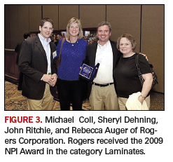
We had the opportunity to speak with Sheryl Dehning, senior marketing communications specialist for Rogers Corporation (
FIGURE 3). Rogers has been particularly active over the past 18 months introducing a number of new products that address the needs of the designers working on mircowave, high-frequency and mixed-signal products.

Fig. 3
How did the idea for the product come about?
Sheryl Dehning: Working closely with OEMs in the Defense/Aerospace industry, we identified the need for an ultra-lightweight dielectric with a very low dielectric constant (Dk).
PCD&F: How long was the product in development and then in beta site testing?
Sheryl Dehning: The product was in development for over a year and spent approximately half a year in beta site testing.
PCD&F: Why is this product important to the PCB industry?
Sheryl Dehning: Ultra-low dielectric constant materials are notoriously difficult to fabricate, RT/duroid 5880LZ combines a unique set of properties: MLB capable/processability, low loss, very low Dk, and lightweight material.
Rogers RT/duroid 5880LZ material is a PTFE composite designed for exacting stripline and microstrip circuit applications. Its groundbreaking filler system results in a very low density (1.37 gm/cm3), lightweight material, making it ideal for high performance, weight sensitive applications such as airborne antennas. RT/duroid 5880LZ laminate has a dielectric constant (Dk) of 1.96 @ 10 GHz, providing the lowest Dk of a copper clad microwave material available today and a very low TCDk of -22 PPM/°C. Additionally, the dielectric constant is highly isotropic (same Dk in x, y, and z directions) and uniform from panel-to-panel and constant over a wide frequency range. RT/duroid 5880LZ is multilayer capable, enabled by a z-axis CTE of less than 46 PPM/°C, and its low dissipation factor extends the usefulness of the material to Ku-band frequencies and above.
For more information on these products contact:
Dow Electronic Materials: Jeffery Tsao, marketing manager, Americas, Interconnect Technology;
This email address is being protected from spambots. You need JavaScript enabled to view it..
Sigrity, Inc: Leslie Landers, VP sales and marketing;
This email address is being protected from spambots. You need JavaScript enabled to view it..
Rogers Corporation: Sheryl Dehning, senior marketing communications specialist;
This email address is being protected from spambots. You need JavaScript enabled to view it.. pcd&f
Kathy Nargi-Toth is editor of
Printed Circuit Design & Fab;
This email address is being protected from spambots. You need JavaScript enabled to view it..


