Glass type does influence skew, impedance and common mode conversion.
As data link speeds increase, so do the problems that affect signal quality. A common tool for the SI engineer is circuit simulation. By modeling the channel virtually, engineers are able to predict waveforms, not only at the receiver, but also at each section of their modeled channel. This level of detail allows us to verify signal detection, as well as to determine the contribution of signal distortion of each section of the channel. To improve or to optimize our system, we identify the sections of channel that produce the greatest signal distortion and make intelligent changes. These changes can include geometric variations, elimination/addition of components or material selection.
One important caveat to circuit simulation is that we must obtain accurate models for each of the components in the channel. Unlike measurements where only a probe location is important, the SI engineer, who produces a virtual channel, must understand the exact path the signal will take. Models for each section must be electromagnetically accurate and reflect the true properties of the system. This is often a difficult task because manufacturing tolerances will vary the true geometry and material properties of each piece of hardware.
Since it is impossible to know exactly how a PCB will turn out, we need to understand what could vary in the manufacturing process– and by how much– and include it in our simulation models. Our goal is to not necessarily predict an exact performance of a channel but rather bound the limits of performance. This typically involves corner studies, where each block in the channel is varied by maximum and minimum potential variation, usually resulting in a substantial number of different models for the same component. For instance, two identically designed transmission lines may have physically different trace widths, trace shapes, dielectric dimensions and dielectric constants.
One often-neglected phenomena of the manufacturing process is the fiber weave effect (FWE). Depending on the materials and construction used, the glass bundles in the dielectric can have a significant effect on transmission line properties. As data link speeds increase, this effect is becoming a more pronounced factor in channel variability. Understanding this effect and the potential signal integrity issues it introduces is critical to designing robust high-speed data links on low-cost materials.
Knowing the potential variability of the glass weave in a given channel will enable a better choice of materials and also bound the impact on signal transmission. We will primarily investigate differential and single-ended microstrip because it tends to have the biggest variations due to glass weave.
In this study, we will limit our investigation purely to the FWE. One of the significant benefits of simulation is that we can control our variables and only change one parameter at a time. In the lab, it is often difficult to distinguish individual channel contributions because we can only measure the total system, and manufacturing variations are also impossible to measure without destroying the test vehicle.
Typical PCB Construction
Printed circuit boards are typically constructed from multiple sheets of laminate material. A laminate sheet can have three basic materials in it: copper, resin and reinforcement (typically glass fabric). At the beginning of the laminate manufacturing process, the resin is in a liquid form. Woven glass fabric is pulled through the resin in a controlled process to fully saturate the cloth. The resin-impregnated glass fabric is then heated to remove volatiles from the resin; this partially cured resin coated glass fabric is known B-stage laminate (C-stage is fully cured), or prepreg. When the resin is heated further, typically under pressure, it re-liquefies, flows and then cures to become a solid material. A laminate core is typically fabricated using one or more plies of prepreg laminated under heat and pressure between two layers of copper foil. The multilayer circuit board is constructed by stacking etched laminate cores, prepreg plies and copper foil for the outer layers, and the material stack is then laminated under heat and pressure to fully cure the prepreg, bonding all the materials together. During the lamination process, the liquid B-staged resin can flow, leaving areas of the board, having more or less resin, somewhat dependant on circuit patterns and glass weave type.
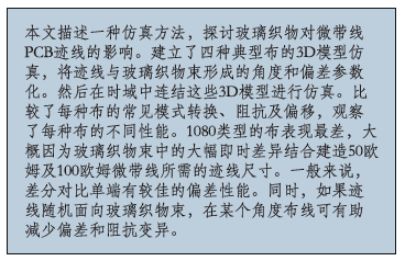
In
FIGURE 1, you can see a cross section of a microstrip trace that has a single laminate sheet that uses a large glass cloth. You can clearly see sections of the dielectric that are mostly glass and others that are purely resin.

Simulation Setup
The most important part of any signal integrity analysis is obtaining accurate models. For this study, we used the 3D field solver HFSS to extract the S-Parameters of the different microstrip configurations. Since 3D simulation is computationally intensive, we will solve only for a short section of microstrip and then concatenate multiple sections together to create a more reasonable six-inch length of transmission line. To combine the models and to perform time domain simulations, we will use Designer with Nexxim.
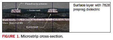
The type of glass cloth used primarily determines the laminate thickness. Different layer thicknesses can be achieved by using different combinations of prepreg.
FIGURE 2 lists buildups for a dielectric supplied by Nelco. The construction column refers to the quantity and types of glass cloth used to achieve the thickness listed at the beginning of the row.

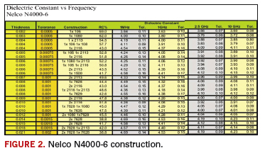
The different glass cloths used for construction will have their own set of dimensions based on type. The glass will have different bundle shapes, thread count and overall thickness.
FIGURE 3 shows six typical glass cloths.

To simulate the fiber weave effect, we created a parameterized 3D model of the glass cloth embedded in a block of resin. A solid object representing each glass bundle was created by sweeping an ellipse along an equation-based polyline. All dimensions of the ellipse and polyline were parameterized so that a single model may be tailored to any cloth type. The rotation was also parameterized, allowing the exploration of different routing angles.
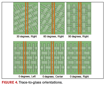
Our investigation explored four typical glass cloth types: 106, 1080, 2116 and 7628. A single glass ply laminate (laminate constructed using only one sheet of prepreg) was used for each of the four test configurations. The 3D model parameters were set based on the dimensions in Figure 3 and as seen in
FIGURE 4. Dielectric constants for the glass and resin were assumed to be 6.0 and 3.5 respectively, as indicated by the Nelco literature.

The 2.2-mil thick rectangular microstrip traces were placed on top of the dielectric models, and both single-ended and differential models were created. The trace widths and separation were parameterized so the impedance would be around 100 ohms and 50 ohms for differential and single-ended traces respectively. Each model varied slightly in length but generally was about 130 mil long. A small section containing only resin was placed at the ends of the traces near the ports to ensure a uniform launch and to aid in accuracy. This small section was automatically de-embedded from the end calculations.
The root cause of the fiber weave effect is the variability of the trace’s capacitance to the nearest ground plane. Glass typically has a much higher dielectric constant than the resin that surrounds it. Because of the glass bundle shape and the trace routing, the capacitance will change periodically based on distance down the trace.
It is impossible to know the exact glass-to-trace orientation during manufacturing, so it is important to understand the limits of the potential electrical variations. Each of the differential and single-ended cloths were parameterized to vary the trace angle and offset from bundle center. The angle was varied from 0° to 90°, in 30° increments. The traces were also offset from the center of a glass bundle to the center of gap with five increments. Figure 4 shows some different orientations of trace-to-glass bundles.
After the 3D models were simulated, the S-Parameters were plotted and inspected for consistency. The individual HFSS models were then concatenated together using the circuit simulator Designer with Nexxim. Multiple blocks were added in series to form a total line length of six inches. Each of the blocks could call a separate HFSS project and access all of the solved parametric data contained within; however, for this study, all circuit blocks referenced the same 3D model and variation. This emulated a length of line that routed perfectly straight and was at a constant angle, offset with the glass fibers. This was done for consistency and to help bound the worst-case line performance.
Please note that our investigation revolves solely around variations in the glass cloth. Random jitter, trace width variations, dielectric thickness variations, calibration and probing effects will all be ignored.
Common Mode Conversion
Mixed mode S-Parameters reliably captures how much common mode is generated from a differential signal in a passive interconnect. Generally, more common mode means more problems– this is especially true when considering EMI. To see the common mode conversion of the different configurations, only a linear network analysis needs to be performed. Of course, the setup is only valid for the differential case. Both the near end and far end conversion were plotted using
EQUATION 1 and
EQUATION 2, where Ports 1 and Ports 3 are the positive and negative inputs, and Ports 2 and Ports 4 are the positive and negative outputs.
SCD11 = 0.5 *(S11 – S13 + S31 – S33) (
EQ. 1)
SCD21 = 0.5*(S21 – S23 + S41 – S43) (
EQ. 2)
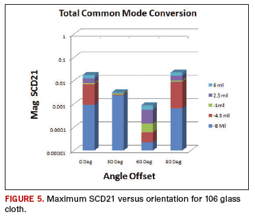
For each of the different cloths, SCD11 and SCD21 were plotted from 0 GHz to 15 GHz for each of the variations. In order to get a sense of how much variation is introduced by the cloth and orientation, the maximums for all variations of the cloths were compared, as illustrated in
FIGURE 5. Surprisingly, there was a very large difference in maximum values for each cloth, depending on the orientation of the trace to the glass bundles.

While the mixed mode parameters provide a good comparison between the variations, it is difficult to determine “how much is too much.” Depending on the system, the common mode current may be well controlled by the planes and isolated from potential radiators. The important takeaway is that there is a significant difference in common mode generated, depending on the glass cloth structure and orientation.
Impedance
To measure the impedance of the different configurations, a standard TDR setup was constructed in Designer. A step response with a 35 ps rise time was injected into the six-inch transmission line. Both differential and single-ended configurations were used appropriately. In order to compare the glass cloths and orientations, a common sample point was chosen at 3 ns, approximately half the electrical length of the transmission line. The Min and Max values for all variations of each cloth were compared.
As you can see from the results in
FIGURE 6, impedance variations are strongly dependent on the type of glass cloth used. Cloth type 1080 showed the most variation, while 2116 had the least. This was true for both differential and single-ended traces. Surprisingly, differential traces showed more variations, even as a percentage of total, than their single-ended counter parts.

Skew
A time domain simulation was again used to capture the skew. A differential or single-ended pulse was launched into a six-inch transmission line, and the far end waveform was measured. The flight time was captured at the exact moment the waveform crossed the 50% threshold. For each cloth, all of the variations were simulated, and the Min, Max, Range and Standard Deviations were compared. The skew per inch was also calculated by dividing the exact length of the transmission line.
Cloth 1080 again showed the most variation. For single-ended traces, it showed a worst-case skew of 4.4 ps/inch. In general, single-ended traces showed much higher impact on skew than differential. This could prove to be problematic for memory applications that use a single-ply, large laminate sheet.
Another interesting observation is the range in flight times based on the angle. Generally, the skew between lines is greatest when the trace is parallel to the glass. An example of this is shown in
FIGURE 7. If we route at an angle to the cloth, the perturbations due to glass are similar, even as we offset the trace. As you can see, the trace routed at 0° has a greater flight time variation than the traces routed at 30° or 60°. This is a similar observation to the common mode conversion case study.

Summary
A simulation methodology was used to explore the effect glass weave has on microstrip PCB traces. 3D models were created and simulated for four typical cloths, and the models parameterized the angle and the offset of the trace(s) to the glass bundles. These 3D models were then concatenated and simulated in the time domain. Common mode conversion, impedance and skew where compared for each cloth type, and different performances were seen for each of the cloths. Cloth type 1080 fared the worst, presumably due to the combination of large instantaneous differences in glass bundles and the dimensions of the traces needed to construct 50-ohm and 100-ohm microstrips. Generally, differential pairs showed better skew performance than single-ended. Also, routing at an angle can help reduce skew and impedance variations, if the trace is randomly oriented with the glass bundles.
Common mode conversion was surprisingly varied between the iterations, and it was high in magnitude, up to 1% of energy. Common mode could present added challenges to EMI mitigation. TDR impedance and skew for the different lines did not seem as disastrous as some other investigations, but be aware the fiber weave effect is only one of many factors that could affect impedance and skew.
PCD&FChris Herrick is technical lead at Ansoft LLC a subsidiary of ANSYS, Inc;
This email address is being protected from spambots. You need JavaScript enabled to view it..
Thomas Buck is a senior technologies with DDI;
This email address is being protected from spambots. You need JavaScript enabled to view it..
Ruihua Ding is a Ph.D. candidate at University of Washington, Seattle;
This email address is being protected from spambots. You need JavaScript enabled to view it..
Ed. note: This article was presented at DesignCon 2009.


