Complex power distribution network design requires accurate analysis tools that are useable by engineers close to the PCB layout process.
The business challenges for electronics companies have remained the same for years: how to produce better products than their competition, with lower development and manufacturing costs and in time to hit the market sweet spot. Today, it’s even more important. With the economy causing budget cuts, designers are being asked to do more, better and faster, often with less manpower.
Today, IC and FPGA suppliers are continually trying to deliver higher density and faster products that consume less power. As they put millions of transistors on chips and run them at higher speeds, the power increases, and the ability for the end product to dissipate the heat byproduct becomes a challenge.
One approach is lower operating voltages. This consumes less power, and they switch faster. If we look back a few years, all ICs ran at 5 V. Today, we see voltages as low as 0.9 V, with many having multiple low voltages on the same IC.
Running at these lower voltages does present some problems. When ICs ran at 5 V, a drop of 0.5 V across your power supply network was within tolerance, and the ICs worked. With voltages at about one volt, you cannot afford a margin of more than a few tens of millivolts and still have working ICs.
In the days of all 5-volt ICs, a PCB designer could allocate one full plane to 5 V and one to ground. The flooded planes delivered good quality power, and we only used two of our layers to deliver that power. The cost of the PCB stayed competitive. Today, we can have PCBs that need to contain many different voltage levels delivered to different parts of the PCB. Gone are the days of allocating a plane for each voltage. The voltage would be clean, but the PCB cost would be prohibitive.
Now power and ground distribution networks must be jigsaw puzzled into the PCB, where a single layer contains multiple, segregated networks.
These complex PDNs pose two DC problems, which if not solved correctly, can adversely affect the cost and reliability of the final product — voltage drop and current density.
As with a signal line, the PDN suffers a voltage drop, as the current flows from the source to the ICs. The more copper in the network and fewer small neck-downs, the lower the voltage drops will be. A conservative approach would be to over-design the network, but this might result in the use of additional layers allocated to PDNs, thus, increasing the cost of the PCB.
Design analysis capability lets you determine the exact DC voltage at every point in the PDN, compare that point to the voltage tolerance of the ICs and identify areas outside of tolerance. The PDN can then be designed to deliver sufficient voltage but without over-design and extra cost.
The second DC issue is current density. High current density produces heat, which can either cause de-lamination of the PCB layers or act as a fuse. This situation may not be discovered but occur in the field, causing a product reliability problem. Again, a conservative approach might result in over-design of the PDN and product cost issues.
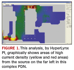
The solution to this problem is to have design analysis tools that can predict the current densities throughout the PDN, as illustrated in FIGURE 1, and compare that with the specification. Select changes, such as a parallel area fill on an adjacent layer connected through-vias, can be made instead of just throwing excessive copper at the problem.

PDNs also have an AC problem that can introduce noise into the system and cause signal integrity problems. When several of the I/Os on an IC package switch simultaneously (drawing a spike of current from the PDN), it has the effect similar to dropping a large stone in a quiet pool of water. And many ICs on the PDN are likely to be switching, giving the effect of several stones in the pool. This turns the PDN into a “transmission plane” (the 2-D analog of a transmission line) and causes reflections that produce EMI.
The easiest and most conservative solution is to throw many de-caps of many values at the problem, but de-caps take up space and cost both procurement and manufacturing dollars. The proper solution is to analyze the PDN and place the right values and numbers of de-caps in the correct locations. This will dampen reflections and keep the PDN noise within tolerance (clean power), while allowing more product functionality in the given space, at a competitive cost.
With today’s complex power distribution network design, meeting the business goals of getting the most competitive product to market, at the lowest product and development cost, in the least amount of time and with limited development resources, requires a power integrity analysis tool that is not only accurate but useable by engineers close to the PCB layout process. These tools are available now and plug into all of the major PCB systems design offerings. PCD&F
Henry Potts is vice president and general manager, Mentor Graphics, System Design Division. He can be reached at This email address is being protected from spambots. You need JavaScript enabled to view it..


