Note: Part 1 ran in the May issue. Part 2 ran in the July issue. All three parts are included here.
PART 1
Electroplating difficulty is measured by board thickness, hole diameter and aspect ratio.
If one thought that electroless copper and other metallization systems were complex, and the deep dark secrets of these systems were shrouded in black magic, this month’s discussions on electroplating will seem like brain surgery.
In this next series of columns, the intricacies of electrodeposition technology and its function of building up the thickness of copper in the through holes and on the board surface will be presented in detail. The function of the active ingredients in the electrolytic copper plating solutions will be presented. Process control limits for the various plating solution components and the effects on deposit integrity will be discussed.
Electrodeposition
In contrast to the classic initial through-hole metallization with electroless copper, the buildup of the conductive layer to a desired thickness in a through-hole is achieved by the electrodeposition of copper. It is understood that these technologies overlap, i.e., that some initial metallization processes use direct electroplating and, conversely, fully additive processes deposit copper solely with the electroless process.
The historic preference for electroplating relates to the lower cost, faster deposition rate, and the generally better metallurgical properties of the electroplated copper. Different chemical compositions of electroplating copper baths have been in use, such as alkaline pyrophosphate baths and acid cupric sulfate baths. Sulfuric acid based compositions now dominating the industry. Improvements have been concentrated on the “throwing copper” of the baths (e.g., their ability to deposit a relatively uniform layer of copper in a through-hole and on the board surface). A shift to higher acid and lower copper concentrations, as well as improved organic additive systems, (brighteners, carriers, and levelers) have demonstrated the ability to improve throwing power.
Several other electroplating processes are used in the fabrication of the printed circuit boards. Tin/lead or tin can be electroplated, and occasionally they can be deposited from an electroless chemistry to act as a metal etch resist. Other electroplated metals include nickel/gold and palladium (also deposited from immersion baths or electroless baths when deposited selectively) to form suitable surface finishes for insertion connectors or component attachment (e.g., wire bonding).
Focusing on the acid copper electroplating process, the first step is the preplate cleaning sequence of acid soak cleaner, microetch, and acid predip. The acid predip is optional and can be omitted if rinsing after microetching is sufficient. However, this only applies when using peroxide sulfuric acid micro-etchants. Use of persulfate based etchants requires an acidic predip. Critical acid cleaner variables are chemical composition, concentration, time, and temperature. Regarding the microetch process, etch depth is the critical parameter, and is influenced by the chemical composition, concentration, time, and temperature. The acid predip, typically the same acid at the same concentration that is used in the plating bath, protects the plating solution from undesirable drag-in, which might adversely affect the composition or concentration of the bath. Thus, the chemical composition of the predip and its level of contaminants are critical.
Critical parameters of the acid copper bath include electrical, mechanical, physical, and chemical variables. Starting with the electrical parameters, current density and primary current density distribution affects plating rate, thickness across the board surface, and the metallurgical properties (e.g., ductility, roughness and color) of the deposit. The current density across the plating surface depends on the rectifier capacity, related anode and cathode sizes, as well as spacing, shielding, cell efficiency, and solution conductivity. The current density distribution across the plating surface depends on several of the previously mentioned factors and, in the case of pattern plating, also on the circuit pattern. The current density in the through-hole depends on the following additional variables:
- Through-hole diameter and aspect ratio
- Replenishment efficiency of plating solution (agitation)
- Throwing power of the bath, which is largely determined by the acid/copper ratio, the organic plating additives, and the level of impurities (organic and inorganic) that interfere with the organic plating additives.
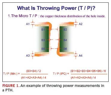
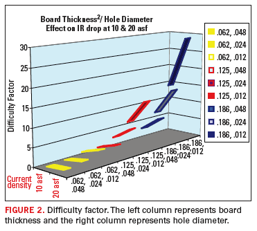
In Figure 1, throwing power is defined for purposes of this and subsequent columns. The actual mechanics of the electrodeposition process, and the influence of process parameters will be discussed in future columns. The degree of difficulty for plating through-holes depends on board thickness as well as hole diameter. For example, given a choice of two holes, both with a 10:1 aspect ratio, the preference would be to design a 100 mil thick panel with a 10 mil via diameter, versus a 200 mil thick panel with 20 mil diameter holes.

Figure 2 underscores the difficulty in maintaining throwing power as the aspect ratio increases. Figure 2 illustrates that the IR drop (or the electrical resistance through the via) increases as a squared factor, while via diameter only effects the resistance (or throwing power) in a linear fashion.

In Part 2, we will continue to explore the electrodeposition process.
PART 2
Advanced technology PCBs require electrolytic copper capable of excellent throwing power and leveling.
With smaller diameter vias and thicker panels, the importance of a high throwing power, high leveling acid copper electrodeposition process takes on added significance. In order for high aspect ratio vias to withstand multiple thermal cycles, the copper plating within the via must be uniform and have optimum physical properties. Additionally, the quality of the copper deposit depends in part on the performance of the initial metallization process that has been previously discussed.
Mathematical Modeling of Plating Uniformity
There are a number of published studies on the subject of plating uniformity in through holes. In these studies, researchers developed models to test plating uniformity. With respect to plated through holes, the models attempted to predict what influence key variables had on plating uniformity. The variables include:
- Mass transport
- Ohmic resistance
- Electrode reactions
- Circuitry layout
Basically, one has to optimize the electrolytic copper process for plating on the surface and in the through hole. Studies indicated that ohmic resistance tended to dominate the plating process with the higher aspect ratio through holes. For example, the ohmic resistance (or voltage drop) can be explained by the following model:

Where E is the ohmic resistance, J is cathode current density, K is solution resistance, d is hole diameter and L is length of hole (board thickness).
As the model shows, the thickness of the panel or length of the hole influences the difficulty of plating by a squared term. In addition, an optimal balance between agitation on the PCB surface and solution movement in the holes was required to achieve a compromise between uniform plating distribution across the panel surface and excellent throwing power in the hole. The model developed by these scientists has been verified time and time again.
Plating uniformity is a continual challenge for through-hole PCB manufacturing and is becoming more difficult with increasingly complex designs. It should be quite clear that plating uniformity is closely influenced by solution chemistry and solution agitation conditions.
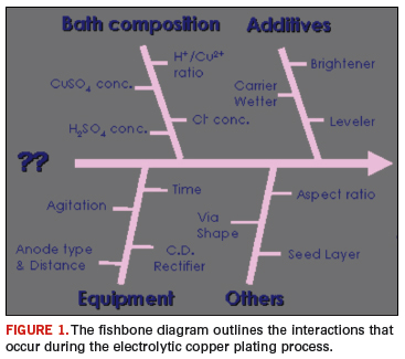
Certainly, understanding the ramifications of the model is critical with respect to plating distribution, throwing power and overall plated through-hole reliability. The factors listed in the fishbone diagram below provide a framework for discussion. These and other variables will be discussed in this and subsequent columns. The fishbone diagram in Figure 1 highlight the numerous interactions that occur during the electrolytic copper plating process.

The function of the basic chemical components in an electrolytic copper bath are listed below:
- Copper Sulfate. Provides source of copper (+2) ions.
- Sulfuric Acid. Provides solution conductivity and anode corrosion.
- Chloride Ion. Plays a synergistic role with organic additives in the brightening and leveling mechanism. Also promotes even anode corrosion.
- Organic Addition Agents. There are a myriad of addition agents commercially available. The function of these additives is to provide a mechanism whereby the copper deposit is plated in a level and ductile condition. Typically, the addition agent package consists of grain refiners, leveling agents and suppressors. For purposes of this discussion, the grain refiner is used interchangeably with the term “brightener.”
- Brightener. The brightener or grain refiner is a member of a class of organic compounds characterized by the designation X-S. The grain refiner contains low molecular weight sulphur (S) and a second atom (X) of high polarity and/or ionic character. Typical brighteners additives are thiourea, disulfides, thiocarbamates, thiocarboxylic acid amides, etc. The “brightener,” by coulombic attraction, forms a layer on the surface where the additive assists in the refinement of the copper grain structure as it is deposited. The structure of the copper deposit is often described as fine grained or amorphous.
- Suppressors. Another component of the acid copper addition agent system will be high molecular weight polyether compounds, surfactants, polyoxyalkylene glycols, and others of similar structure. This additive acts as a suppressor by converting an unevenly distributed stationary cathode diffusion layer into a more evenly distributed layer. This action reduces the variation in copper deposit thickness across the surface caused by uneven diffusion paths that exist in the absence of a suppressor. In other words, the suppressor acts to prevent overplating in the high current density areas of the printed circuit board.
- Leveler. A third component of the additive system is referred to as a leveler. The leveler is highly polar, and by its nature adsorbs preferentially near the most negatively charged sites of the cathode (PCB). This action slows down the charge transfer of the copper ions to copper metal, thus slowing down the plating rate in those areas typically considered high current density areas. Basically, if over plating distribution and throwing power is to be improved, this is a necessary action.
In Part 3, we will look further into the electrochemistry of plating using the various mathematical models for determining plating uniformity.
PART 3
Plating cell design can minimize the effects of primary current distribution.
In the previous column, a broad overview of copper electrodeposition was presented. In this month’s feature, the functional aspects of electrodeposition will be presented in greater detail. It is critical to obtain a fundamental understanding of the plating process, including an in depth knowledge of the various additives, organic as well as inorganic. Additionally, mechanical factors such as agitation, operating temperatures, cathode current density and anode placement have influence on the plating process.
As printed wiring board designs become increasingly more complex, with smaller diameter vias and greater panel thicknessess, the engineer faces a more difficult task with respect to optimizing plating distribution; this includes throwing power and the physical and cosmetic properties of the copper deposit. Optimizing the operation of the chemistry is a big task. The additives in the chemistry interact with the various mechanical aspects of the plating system. The rectifiers, anode to cathode relationship, filtration, agitation and plating by-product build-up influence the plating distribution and overall quality and reliability of the copper deposit as well.
Taking this a step further, achieving plating thickness uniformity is largely dependent on primary and secondary current distribution.
Primary Current Distribution
Primary current distribution involves the main influencers of plating uniformity; the plating cell design and geometry, anode and cathode spacing, and the size and shape of the anode and cathode. The pattern image of the PCB will also influence plating uniformity. However, the less uniform a plating pattern (according to primary current distribution), the greater the variation in the plating thickness across such a pattern. It is commonly understood that PCB patterns that are very uniform in the layout of the circuit features exhibiting a uniform plating area across the panel will plate with minimal thickness variation. However, designs that exhibit ultra-uniform circuit layout patterns are not all that common.
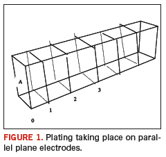
Certainly, this concept can be explained by looking at simple plating applications. In one such application, assume the plating is taking place on parallel plane electrodes as depicted in Figure 1. This is often referred to as the mathematical concept of equi-potential surfaces. Looking at the parallel planes in Figure 1, it is easy to see that current flowing between adjacent parallel electrodes is constant across the electrode surfaces. Thus, the length the current flow is equal.

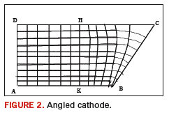
It is easy to see that the potential between two parallel surfaces is constant across the surface. For two parallel electrodes, the current at any point on either electrode is equal. Thus, plating thicknesses would be equal. Figure 2 illustrates what would happen if the electrodes where rotated or angled with respect to one another; the equi-potential surfaces would no longer be parallel to each other.

The above figure is similar to the Hull Cell Testing concept, whereby the cathode is set at an angle from the anode to simulate varying current densities. When one of the electrodes is angled in such a fashion, the lines of current flow become more tightly spaced at the angled end. (see area AKB versus DHC in Figure 2). Due to the angle of BC, point B is closer to the AD electrode than is point C. Since the lines of current flow are always perpendicular to the to the equi-potential surface, the lines of flow become more tightly spaced at the angled end, resulting in a current density (i.e. plating thickness) variation across the BC surface.
While this explanation is somewhat a simplification, one can see that potential theory does apply to plating cell design and anode/cathode configuration. Engineers must consider anode to cathode relationships with respect to size and spacing.
In the next installment of “Positive Plating” the subject of anode to cathode spacing and secondary current distribution will be discussed in detail. In the meantime, stay positive. PCD&F
Michael Carano is vice president for OM Group, Inc. and can be reached at This email address is being protected from spambots. You need JavaScript enabled to view it..


