Electronics companies across markets are hopping on PoP.
When land is limited, builders construct high-rise condos and apartments. When board real estate is limited, packages also go in the z-direction. Some of the high growth areas include stacked die CSPs and package-on-package (PoP). Next in the progression of technologies moving in three dimensions is through silicon via technology for stacking silicon devices.
Stacked die CSPs. Driven by portable applications that require extremely small form factors, shipments of stacked die packages have grown dramatically in the past five years. Stacked die inside CSPs are found in mobile phones and a variety of consumer products such as cameras and camcorders. More than 2.5 billion packages were shipped in 2007, and the number is expected to grow in 2008.1
While the first applications had two stacked die, the average number of die in a stack is increasing. Shipments of stacks with four or more die are common, and some companies have moved into production with stacks of six to nine die – some containing both logic and memory. Hynix has demonstrated a 20-chip memory stack in an R&D project. Typical die thicknesses in production range from 75 to 125 µm for conventional die stacking. Stacked die are still largely wire bonded, but flip chip use is beginning to increase.
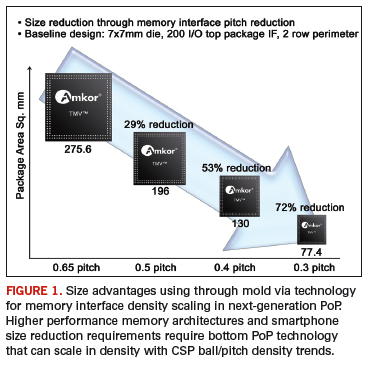
Package-on-package. According to Amkor, PoP is one of the company’s fastest-growing packages, and may be one of the industry’s, too. With almost 150 million top and 150 million bottom packages shipped last year, and an installed base of more than 150 mounting systems from a variety of companies, Amkor is probably right. Today’s applications include mobile phones (the largest), digital cameras, and MP3 players. Future applications include medical products, laptops and ultra-mobile PCs. Amkor has developed a through mold via technology for next-generation PoP. It will scale with trends in the top memory package as pin counts increase, pitch transitions below 0.5 mm, and the solder balls move beyond two rows to multi rows. The new process follows a standard mold array process flow, but uses a laser to open vias (Figure 1).

Stacking die inside the package results in the thinnest package with the highest board-level reliability and lowest assembly cost compared to other z-direction packages. This package however, is not always the best choice when a logic device is added. PoP was developed because it offers several advantages over stacked die packages, especially where there is a need to stack logic and memory. Each package can be individually tested before stacking. Two packages from different suppliers can be stacked and it is easy to change memory capacity. The cost of a known good memory die may be almost the same as a packaged die. This can decrease the margin of the stacked die supplier. If known good die are not used, yield issues are compounded.
There are some disadvantages to PoP. Package cost may be higher for the PoP configuration than for stacked die CSP because there are two substrates rather than one.
Co-planarity of the two packages, especially during reflow, was an issue in the early days, but a tremendous amount of work has been done to alleviate this problem. Substrate warpage has been the key issue, and a number of companies have developed solutions. Both the top and bottom packages must be optimized. The liquidus/reflow temperature is the most critical in the process. Amkor has conducted extensive package warpage optimization studies varying both substrate thickness and mold materials. Substrate design rules (routing), core thickness, copper ratio and prepreg materials have been optimized. Die thickness and material properties also had to be optimized, while mold compound filler size, CTE, Tg, shrinkage and thickness had to be carefully specified. Amkor found that a very flat top package is key to good stacking yields.
Several companies, including Henkel and Indium, have introduced flux materials. Henkel’s epoxy flux, for instance, shows good connectivity and increased reinforcement.2
While there have been concerns over package height, which is thicker than the traditional stacked die package, solutions are being developed. These include embedding devices in the substrate, thinner substrates and concepts such as Tessera’s MicroPILR package. The top package typically contains high capacity or combo memory devices. The bottom package typically contains a high-density logic device. Body sizes range from 10 x 10 mm to 15 x 15 mm, with bottom-side ball counts ranging from 240 to more than 400, and package interconnect ball counts ranging from 104 to 160.3
To achieve small package bodies, an increasing number of companies use flip chip inside the package, especially for the bottom die in a package of a PoP. Flip chip reduces pitch for the top package of a PoP, and improves electrical performance for devices such as baseband processors by delivering power directly to the processor core, along with reduced IR drop and reduced EMI.
TSV: The ultimate in 3-D. TSV technology permits devices to be placed and wired in the third dimension. 3-D TSV adoption promises higher clock rates, lower power dissipation and higher integration density. The technology will be adopted in many applications because it solves issues related to electrical performance, memory latency, power, and noise on and off the chip. For some applications, a high-bandwidth memory interface to the logic has been the main driver for the technology’s development. Both logic and memory device applications are expected to begin within a few years. The addition of DSP to image sensors is also anticipated in future camera module versions. There were more than three dozen papers on 3-D packaging at the Electronic Components and Technology Conference in May 27-30, and the sessions were packed.
Even with 3-D ICs’ advantages, there are several challenges to the adoption of 3-D architectures. These challenges need to be overcome for the technology to see widespread adoption.
- Commercial availability of EDA tools and design methodologies.
- Thermal concerns due to increased power densities.
- Test, especially for repartitioned logic.
The TSV market will be established when the benefits justify the cost, and on a case-by-case basis. While through vias are used in image sensors for camera modules today, other applications will take time. TSMC’s recent TSV announcements as part of its Open Innovation Platform will aid the adoption. TSMC is working with customers on design software and has introduced a SPIC tool design kit. The first technology is a post through-silicon via technology capable of 140 µm pitch. By the end of 2009, TSMC will offer a post TSV technology with 60 µm pitch and, sometime in 2011, 17 µm pitch inline capability.
Movement in the z-direction continues and a variety of solutions will remain. Stacked die CSPs will continue to see high growth. PoP adoption will expand as many system makers hop on the bandwagon. The ultimate silicon stacking, 3-D TSV, will see widespread adoption as some of today’s key issues are resolved. PCD&F
References
1. TechSearch International Inc., Advanced Packaging Update: Market and Technology Trends, March 2008.
2. B. Toleno Ph.D., and D. Maslyk, “Process and Assembly Methods for Increased Yield of Package On Package Devices,” IPC Apex Proceedings, April 2008.
3. F. Yuan, Ph.D., and R. Crisp, “Design and Modeling of High-Speed, High-Density 3-D CSPs and Memory Modules,” Circuits Assembly, April 2008.


