Reliable lead-free assemblies require a collaborative approach that
optimizes the PCB design along with specific base materials and known
fabrication processes.
With the advent of RoHS companies have been forced to restrict the
amount of lead in the electronic equipment produced. To comply with
these guidelines, there has been a move toward the use of lead-free
solders for PCB assemblies. Most lead-free solders require higher
assembly and rework temperatures. Tin-lead solder assembly has
historically used temperatures that did not exceed 230ËšC. but the
typical soldering temperatures required for lead-free solder range from
245 to 270ËšC. The extra 15ËšC to 30ËšC required for lead-free assembly
has been demonstrated to reduce the reliability of PCBs, and this is
expressed as increased failures at assembly and a reduction of the
field life in the end use environment.
The ability
of PCBs to survive multiple assembly cycles has become a concern in
high-end applications (high layer count and aspect ratios, thicker
constructions, reduced grid and hole size, complex/multiple
interconnections, etc.). Following a simulated lead-free assembly and
rework on representative test coupons, a 50% reduction in reliability
has been commonly demonstrated even in well designed, well fabricated
PCBs made with high reliability lead-free compatible materials. Common
failure modes like barrel cracking still dominate, but material
degradation has now become a significant influence, and can confound
the reliability results. Material degradation has a number of
detrimental effects, the primary reliability effect being the
artificial extension of thermal cycles to failure (CTF), due to the
stress relieving influence of internal delamination. In addition,
material breakdown provides a potential path for the growth of
conductive anodic filaments (CAF) between adjacent features in the end
use environment. Long-term impact of delamination is a potential change
in the electrical characteristics of the PCB, including impedance
values.
Testing Methodologies
Preconditioning
is a simulation of the thermal excursions experienced by the PCBs in
assembly and rework. Assembly simulation is typically three thermal
cycles to the maximum assembly temperature, while assembly and rework
simulation is five or six thermal excursions. Preconditioning is
achieved by processing representative samples through assembly ovens,
or by heating samples on equipment that simulates the assembly thermal
profile. As long as the preconditioning is well controlled, both
methods produce similar results.
In reliability
testing, thermal cycling is continued until there is a 10% increase in
bulk resistance in any circuit, or until end of test at 500 cycles.
Coupons tested “as received” are considered the control sample and the
CTF is the sample’s entitlement. Entitlement establishes the relative
robustness of the sample. It is the sum total of all reliability
influences affecting the sample, including quality, thickness and
uniformity of the electrolytic and electroless coppers, robustness of
material, design influences and other fabrication and assembly process
variables. Preconditioning reduces the entitlement of the sample, and
the more aggressive the preconditioning, the fewer thermal cycles to
failure. Table 1 demonstrates reductions in mean CTF
(tested at 150ËšC), based on an “as received” performance of 500 cycles,
and illustrates the anticipated degradation in CTF commonly measured
after tin-lead and lead-free preconditioning.

This
reduction in cycles to failure is observed when there is no significant
material degradation expressed during testing. Frequently, samples that
have delamination express increasing CTF in response to more aggressive
preconditioning, giving artifact CTF results. Delamination that extends
cycles to failure appears to be stress relieving and, as a result,
reduces the damage accumulation in the metallic interconnect structures.
On
occasion, delamination reduces cycles to failure, but this is
infrequent. Delamination that reduces cycles to failure appears to
increase the stress in the interconnect structure. The delamination in
the dielectric aligns with cracks in the barrel of the PTH. It appears
that stress is focused to the sidewall of the plated barrel, and may
cause catastrophic failures in just a few thermal cycles. This somewhat
rare occurrence is described as stress focusing delamination. In the
majority of cases delamination stress relieves samples, stopping or
slowing down the propagation of copper cracking in the plated through
hole, and the internal innerlayer connections, which would have
occurred in response to the higher z-axis expansion of the dielectric
material.
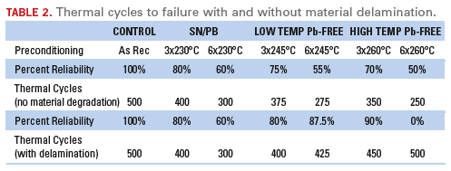
A typical reliability evaluation, where delamination is expressed in the data, is shown in Table 2.
Note that with delamination present in the samples, the cycles to
failure increases in response to more aggressive preconditioning. The
samples tested “as received” and those exposed to six cycles of
preconditioning to 260ËšC both show a CTF of 500 cycles (no failures by
end of test). This increase in CTF as a response to more aggressive
preconditioning is counterintuitive.

Recent
studies have confirmed that not only delamination, but also other types
of material degradation artificially extend CTF. Established IPC
standards consider obvious delamination a condition to be rejected.
Delamination is unacceptable in electronic products for a number of
reasons, including the degradation of electrical attributes by reducing
the dielectric properties of the material. One of the concerns is that
delamination provides a path for conductive anodic filament (CAF)
growth that can occur over time in the end use environment.
Material
degradation is not easily observed by inspection, even with
magnification. Many times delamination is present in PCBs or test
vehicles that show no signs of discoloration or material deformation.
Internal delamination that is not apparent externally may be found by
microscopic examination. The microsection method of delamination
inspection suffers from two disadvantages, first, microscopic
evaluation is expensive and time consuming, forcing the sample sizes to
be small, and the second even greater limitation to this method is the
random nature of delamination. Delamination may be present in discreet
areas and not continuous throughout the PCB or coupon. This sporadic
nature of delamination can confound microscopic evaluations and lead to
false positive conclusions.
An electrical,
non-destructive method for detecting material degradation has been
developed in response to this problem. In order to determine if
material degradation had occurred within the construction, circuits
were included in reliability test coupons (enhanced IST test coupons),
which could detect material changes across the entire sample. Changes
in capacitance were measured between internal planes before
preconditioning or testing (to establish a baseline), after
preconditioning, and at end of test. Relative changes in capacitance
occur when materials are degrading. Not only can this method discern
material degradation, it can also measure the physical changes in
materials in response to thermal cycling.
Armed
with an objective method for determining which test samples had
material changes, microsections were processed and material conditions
were observed. Although microsections are random by nature and limited
to viewing only a small area of a sample, a strong correlation was
found between electrical changes and the presence of material
degradation. Studies conducted over the past five years have
established that a 4% change in capacitance (on specifically design
coupons) demonstrates that material degradation has occurred. This
method confirmed that, when present, delamination was extending thermal
cycles to failure in most test groups.
In a
tin-lead application high reliability materials generally do not
exhibit degradation. In a lead-free application, even high reliability
and lead-free capable materials can exhibit significant degradation. It
is significant in that the degradation is observable electrically and
can be found upon microsection evaluation.
Since
there was a new method for identifying the presence, location (layer)
and degree of material degradation, knowledge of failure modes by means
of microsection analysis was advanced. Thermal cycles to failure
analysis, including damage onset and acceleration, were now being
evaluated against the presence and onset of delamination. It became
possible to identify delamination and other material conditions that
influenced reliability.
One of the challenges in
discussing material failures was the lack of a common vocabulary.
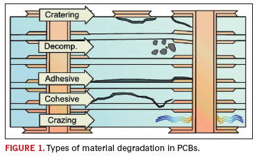
Material degradation may be categorized in five often overlapping
conditions; adhesive delamination, cohesive degradation, crazing,
material decomposition and cratering as shown in Figure 1.
These definitions may be unique to PCB fabricators and have different
connotations in other disciplines. For the purposes of this article the
following definitions apply.

Definitions of Material Degradations:
Adhesive Delamination. This
condition is described as a physical breakdown between two laminated
layers. This type of delamination occurs between the B-stage and copper
foils, the B- and C-stage layers, or epoxy glass fiber bundles. This
type of delamination is an interfacial type failure where cracks occur
between laminated layers, or along glass bundles (not individual glass
fibers). This failure is expressed as a crack proceeding down
epoxy-to-epoxy bonds, epoxy-to-copper interfaces or epoxy-to-glass
bundles. In a cross section, the crack is long, mostly horizontal and
ends in a thin point. A top-down view of the delamination between
laminated layers or copper may show a bubble or blister. Adhesive
delamination along glass bundles may appear to be square or have a
cross or X shape corresponding the knuckles of the woven glass.
Although
most material degradation is a result of many influences, the general
opinion is that adhesive delamination is predominantly a mechanical
failure. Aggressive out-gassing of volatiles (moisture or solvents) may
be the cause for this type of failure. This failure mode is accelerated
by problems in copper surface treatments (oxide or conversion coatings)
or surface contamination on traces and particularly on internal pads
and planes. Adhesive delamination may result when the lamination
process has been compromised, when B-stage materials have exceeded
shelf life or been improperly stored, or where the press cycles
preheat, pressures, cure times or cooling rates are set incorrectly.
Drilling may also play a factor in adhesive delamination. Cracking
along glass fibers may provide a place for aqueous substances to
accumulate prior to electroless copper deposition. These cisterns offer
storage sites for liquids that vaporize during high thermal cycles.
This
failure mode may be expressed in multiple boards from the same lot.
Isolated blisters, pink ring, measling, and large internal material
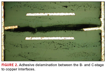
separations are usually a reflection of this failure mode. Figure 2 shows adhesive delamination between the B-stage and C-stage interface and copper surfaces.

Cohesive Degradation. This
condition, commonly described as cohesive delamination in the
electronics industry, may be a misnomer in that it implies lamination
is involved in the failure mode. A cohesive failure occurs within the
base material, but is not implicitly associated with a laminated
interface. Cohesive failures may be described as a breakdown of
material within the B- or C-stage layers of the dielectric. This
failure mode appears to be a degradation precipitated within the epoxy.
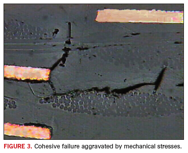
A chemical degradation is most likely the dominant influence in
cohesive failure, though it is undoubtedly aggravated by mechanical
stresses like out-gassing of volatiles (Figure 3).

This
failure occurs when the forces exceed the strength of the material.
Failures occur when either the forces are increased, or the material
loses strength. It appears that, in some instances of cohesive failure,
the failure may occur over time at an isotherm, which suggests the
failure may be precipitated by a loss of material strength. One of the
early descriptors for a PCB was “organic wiring boards,” because the
epoxy is an organic based chemistry that can degrade over time, even at
ambient temperatures. There is a tendency to think that the increased
forces applied to the PCB in lead-free assembly are causing failure.
Note that we are not differentiating between normal and shear stress,
but rather the combination of all forces. It is more likely that
material degradation is working in concert with increased stress, which
results in catastrophic failure of the material. Lead-free assembly and
rework may initiate material damage, which can develop further over
time.
In cohesive failures, cracks propagate across
the materials and are not limited to a material interface. The crack
may change directions producing sharp angles, have an irregular
thickness and end in blunt points. The crack may follow glass fibers
and then cross into resin rich areas of the dielectric. The crack may
be oriented in a horizontal or vertical plane and traverses between B-
and C-stage layers. This failure mode maybe accelerated with
out-gassing volatiles, but may not be presented as a classic blister or
bubble shape. These failures also contain a mechanical component in
that a number of specific design attributes (e.g. grid spacing below
0.040 inch, multiple central planes, heavier copper planes, etc.) tend
to be more prone to this type of failure.
Crazing. This
condition may be described as a separation between the epoxy and
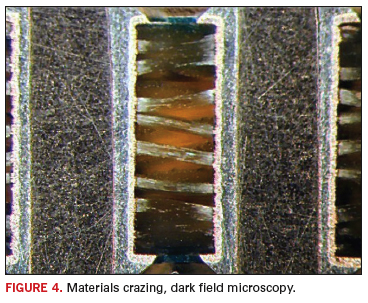
individual glass fibers. This is a more insidious failure mode, in that
there are no obvious visible cracks, but it can be seen as light
refraction observed along glass fibers that are parallel with the plane
of the microsection, as seen in Figure 4. There is a
reluctance to label this condition as delamination, but the effects are
similar. Capacitance changes are observed if this condition develops or
increases in response to thermal excisions associated with assembly,
rework or reliability testing. Dark field microscopy may be useful to
better visualize the magnitude of glass to resin separation.

The
light refraction appears to be due to a small separation of the epoxy
and the glass fabric. Viewed end on, the glass fibers appear to have
black lines around bundles or individual fibers that present as
crescent shaped lines. This failure mode can extend CTF in reliability
testing, but does not accelerate failures.
Crazing
is thought to play a role in CAF type failures by providing a path for
electro-chemical migration. The size of these cracks promotes capillary
action if liquids are present. If crazing occurs before aqueous
processes during fabrication, then liquids may penetrate along the
glass fibers. This situation is further exacerbated by the presence of
an electrical bias, which can cause the migration of ionic
contaminants, bridging between adjacent features. This condition is
implicated in field failures that are developed over time, particularly
when there is high electrical bias in a humid environment accompanied
by thermal cycling.
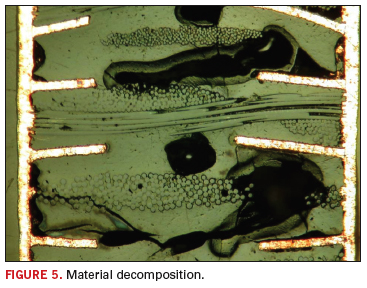
Dielectric Decomposition.
This failure mode is rarely expressed in reliability testing.
Dielectric decomposition presents as a charred material. The boards or
coupons may look dark brown to black, and in extreme cases carbonized
balls may be present beside the vias as shown in Figure 5.
In microscopic examination, the material presents as round voids
resembling bubbles, and there is extreme deformation of copper traces
and pad rotation. Out-gassing is obvious, in that the material looks as
if it has boiled. Surprisingly, circuit conductivity may not be
degraded by material decomposition if the internal interconnections
(barrels and copper posts) are well made.

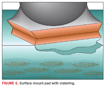
There
is a fifth material condition that is not found by capacitance testing
but should be noted. The condition has been described as “cratering,”
where a surface mount pad develops a crack in the butter coat (resin
rich area) on the surface of the material (Figure 6).
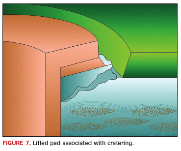
The failure mode is created when the pad and attached material break
away from the surface of the board. This failure mode is associated
with an interaction between the PCB, components and assembly processes.
Another example is the case where the plated through hole has lifted
pads (Figure 7). The area where the dielectric remains attached to the lifted copper may be related to this failure mode.


Material
degradation can be created during assembly, during rework, or thermal
cycling occurring over time in the end use environment. Some materials
that survive lead-free assembly and rework in a product that is less
complex, such as lower layer counts and low aspect ratio construction
PCBs, may fail in high layer count, high aspect ratio applications. In
general, material degradation is more likely to be found in products
designed with a thickness greater than 0.075 inch (1.9 mm), with high
layer counts (12+), higher densities (less than 0.040 inch or 1 mm
grid) and high aspect ratio vias (5 to 1 or greater). There is an
increased vulnerability for delamination in PCBs constructed with
sequential laminations (two or more lamination cycles). This may be due
to internal dielectric layers being exposed to multiple curing cycles.
PCBs, fabricated with high speed materials, and in low loss and
elevated frequency applications are also more vulnerable to material
degradation associated with lead-free assembly.
The common
industry response to material degradation has been to bake boards
before assembly and rework. The baking is done in an effort to remove
volatiles, specifically water. Traditional low temperature (105ËšC)
baking to remove water has demonstrated limited success. Aggressively
applied, baking may further degrade the dielectric material. Aggressive
baking can also degrade the surface finishes making soldering
problematic. Excessive baking by either higher temperature or extended
times may be considered another thermal excursion, adding to the
degradation of the material prior to assembly and rework.
The
best approach to meeting the reliability challenges of lead-free
assembly and rework is to achieve a balance in the fabrication process,
the material used, and the PCB design. Optimizing these three
influences may produce synergy for extended reliability in a given
application. Each PCB is unique by design, by the fabricators processes
and by the materials used. What is reliable in one application may not
be reliable in another. Each application requires objective evaluation,
based on experience and confirmed by testing, to meet the lead-free
reliability challenge. PCD&F
ACKNOWLEDGEMENTS
Appreciation is extended to Bill Birch, Jason Furlong and the team at PWB Interconnect Solution Inc. Ottawa Ontario Canada.
Paul Reid is Program Coordinator at PWB Interconnect Solutions, in Ottawa, Ontario, Canada; This email address is being protected from spambots. You need JavaScript enabled to view it..


