PCB design bottlenecks are reduced using customized tools.
Faster time to market is crucial in the development and
manufacturing of every new product. Many studies indicate that there is
a relationship between project profitability and success, and the time
it takes to get from the original idea until the product is available
in the market. All groups involved in the development of a product are
responsible for assessing how they can contribute to shortening a
product’s time-to-market. This article offers an original solution
applied during PCB design that significantly contributes to the
reduction of work time the process takes to get a product to market.
Today’s
competitive market poses not only technical challenges, but also
business challenges to engineers and product developers alike. On the
technical side, new technologies are constantly emerging and product
complexity increases, challenging R&D engineers who are required to
obtain better performance from their products. On the business side, in
today’s market when a product so quickly becomes obsolete, it is
essential to shorten project times to achieve the goal of minimum
time-to-market (TTM).
PCB design sometimes can cause
a bottleneck in the project development cycle. Both the PCB fabricator
and the assembly company use the output of the design process. In fact,
this stage finalizes hardware development in the project and is the
first step in PCB fabrication and assembly. The electrical design
process sometimes takes longer than planned, shifting pressure to the
design bureau. Effective, fast processes at this stage will reduce
design time, thus contributing to improved TTM and lower NRE costs.
PCBs
are designed using Electronic Design Automation (EDA) software. This
software consists of a set of elementary commands for executing a
design, but also is equipped with powerful customization tools that
enable users to develop dedicated applications using advanced
programming languages, which shorten both processing time and overall
project time.
Despite the differences in every design
project, there are actions throughout the design process that are an
integral part of each project. The content of the action may be
different from project to project, but the work methodology is
identical. For example, near the end of the design process, it is
necessary to prepare the legend pattern that will be screen printed or
inkjet applied onto the PCB. The content of this pattern will differ
from board to board, but the method for executing this work is always
the same. In this case, it would be worthwhile to develop auxiliary
software that could be used by PCB designers for executing this action.
Today, EDA tools generic functionality can
effectively cover 90% of the design of a PCB. The remaining 10% is the
key to success, and can be achieved by the full integration of
customized tools.
The following are some examples
of service programs developed using the Skill language, which are
applied in the Cadence Allegro PCB work environment. All programs run
using the editor’s original toolbar, which has been expanded for this
purpose.
AutoText Orient facilitates
the automatic global or local orientation of text on the PCB based on
the decision of the designer concerning the relative angle and area
that needs to be altered. The program significantly improves the
definition and assembly of screen printing on the board. Instead of
manually defining the printout on each component, the application
analyzes the state of the existing text in terms of orientation and
turns it automatically, at the click of a button, based on the user’s
request. In PCBs with high pin count – over 10,000 for example – this
translates to a savings of several workdays.
Producing
the Gerber files at the end of the PCB design process that is used for
transferring the PCB design to production requires significant time and
accuracy on the part of the designer. Auto Gerber is
a service program that produces Gerber files at the click of a button,
based on the layer order defined by the designers. Designers have a
dynamic graphic interface available that displays the internal and
external layers of the board, enabling them to select the relevant
layers for creating the Gerber files. This application saves 98% of the
time required to create Gerber files at the end of the design phase,
and prevents potential errors in the manufacturing of the PCB.
Check Padstacks
is a service application that verifies the accuracy of the values of
each pin in the PCB, as compared with values in accordance with
IPC-7351 and IPC-2221/2. Recommended golden values in these standards
constitute the database for the service application. Values checked
include pad size, paste mask, solder mask, thermal relief and more. The
application was written in Skill, with data processing in Perl. It
prevents potential errors when defining footprints and ensures that the
PCB will be produced and assembled quickly and smoothly, with zero
faults in the determination of the components library.
A block is defined as a group of components that repeat themselves. Copy Block
is used to place identical blocks on the PCB and to correctly place
components on each block. This eliminates the need for component swap
in each block. After placing the first block, the program scans the
netlist and schematic PDF to identify matches between components and
blocks. Since the configuration of the PCB frequently consists of
functionally identical parts, Copy Block saves time during PCB design.
The program is written in Skill and is based on data deriving from the
netlist and schematic PDF files. Data is processed in Excel VBA.
Another example of a customized application is BGA Auto Grid,
which automatically defines the grid of BGA components based on the
pitch between pins. The program enables the accurate and rapid
placement of small components like 0402 and 0201 packages, which must
be placed at the closest possible distance to a BGA’s legs in order to
obtain better filtering, clock resistance, etc. BGA Auto Grid saves
substantial time in component placement, as it would no longer be
necessary to manually measure the distance between these small
components and the vias. Further, it ensures that the components are
assembled accurately between the vias.
Requirements
for these applications come not only from PCB designers, but also from
customers and development engineers, who sometimes are required to
prepare dedicated designs. The programs are adapted to the nature of
their work and are aimed at making development and design processes
effective. For example, a customer’s footprints library may use
different symbol components with identical names. This is a result of a
non-uniform definition of components in the drawing tools. A request
was made to write a program in Skill to compare components with
identical names and find the difference between them, in terms of the
critical parameters for PCB design, such as height, or the padstacks
that were used to prepare them. This is how Compare Two DRAs was born.
The program produces a report showing definition of symbols (height,
distance between pads, etc.).
Another advantage in
the use of customized programs is a reduction in malfunctions during
the design process. Instead of the designer executing actions manually,
they are automated in the service programs, thus minimizing human error.
The
following are two examples of projects demonstrating the savings
obtained using these customized applications. PCB A was manufactured
without the use of these auxiliary programs. PCB B, on the other hand,
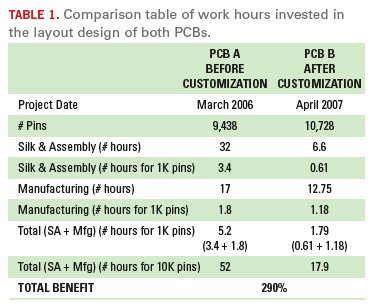
was designed using many of the 22 applications developed. Table 1
shows the work hours invested in the design of both cards. In each one
of the design phases, the number of invested hours was measured. In two
stages of the design process – silk and assembly (SA) and MFG
(preparation of the manufacturing file), use of the programs
significantly reduced working time. For example, SA activities in PCB A
took 32 hours, whereas in PCB B it took only 6.6 hours. For a reliable,
accurate measurement, the hours invested in these two phases were
normalized for each of the projects. A summary of the results
demonstrates that the accumulated savings obtained by the use of these
programs reached 290%!

In a
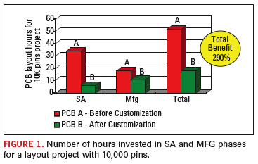
project with 10,000 pins, timesavings reached 34 hours (more than 3
work days). In a project with 20,000 pads, the savings reach 66 hours
(more than a work week). Figure 1 graphically depicts the number of hours invested in SA and MFG for a project with 10,000 pads.

In
summary, time-to-market is crucial to the success of an electronic
product. An evaluation of all stages of the lifecycle of a prototype,
and locating the areas in which it is possible to save time to make
processes more efficient can significantly improve TTM. This article
presented a proven method for shortening PCB design time by using
dedicated customized software applications implemented in the EDA tool.
PCD&F
Arbel Nissan is COO of CircuTec; This email address is being protected from spambots. You need JavaScript enabled to view it..


