The assembly drawing should specify process-related issues.
The processes involved in eliminating board defects cut a wide swath
through design, fabrication, and even assembly. Along the way,
experience and know-how play pivotal roles because solutions to many
defect-prone PCB areas are not covered in textbooks. PCB defects run
the gamut, for example, from deteriorated RF signals resulting from
inappropriate shielding to incorrectly structured boards due to sketchy
or ambiguous fabrication notes, and on to miscalculated thermal
profiles, creating BGA, CSP or QFN-based solder defects or flaws.
Eliminating
board defects starts with the designer. Their experience level and
design-for-assembly (DfA) knowledge has a direct bearing on the number
of defects and flaws detected at PCB assembly. Certainly, the designer
may have a keen sense for design, but if they don’t know how assembly
and manufacturing work, have a firm grip on its processes and a good
understanding of assembly equipment, the PCB design is likely to
experience assembly issues.
For example, on paper,
an RF design looks exactly the same as any other PCB design. However,
in an RF design, a multiplicity of small differences, intricacies and
issues demand careful attention. If not properly addressed at the
outset, they subsequently become defects, which can keep design
engineers busy debugging and trying to eliminate those defects.
Defects
can be created in an RF design in such areas as an improperly designed
antenna, signal deterioration at an unacceptable rate, exceptionally
high noise resulting from poor shielding, improper dissipation of EMI
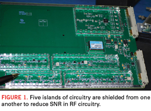
from RF signals, and lack of attention to line-of-sight aspects. Figure 1
shows a board with five islands of circuitry shielded from one another
to reduce signal-to-noise ratio (SNR) in the RF circuitry, and thus
avoid defects.

The designer
must also concentrate on segregating signals to make sure signals of
one particular frequency are properly separated from those of a
different frequency. Otherwise, crosstalk may be created. A savvy PCB
designer incorporates these and other RF design considerations, thus
avoiding RF board defects at assembly and manufacturing.
Board
fabrication and assembly undergo various processes and machines.
Particular attention is crucial in these areas to avoid defects. Lack
of PCB layout experience, for example, can lead to placing BGAs on a
board’s bottom side, although there is plenty of space topside. In a
situation like this, the assembly process is duplicated with two setups
for pick-and-place machines and another two processes for reflow, plus
using ancillary fixtures to ensure those BGAs are protected when
through-hole components undergo reflow. There is nothing wrong with
placing BGAs bottom-side, but if this PCB design and placement were
done correctly, it would have eliminated defects and avoided creating
the basis for future failures.
In cases like this,
when only one side of the board is used for BGA placement, the need for
using epoxy for reflow is eliminated, as is the need for a wave solder
fixture.
An assortment of other defects also arises
from machine limitations, incorrectly designed in tolerances, and board
spacings. DfA takes into consideration physical, height, length, and
package-related limitations. If a board is highly complex with 0201 or
01005 packages, and tight assembly processes are not specified,
multiple board defects can result, such as tombstoning, skewing of
components, and inactivation of flux with solder paste.
A
designer also has to know the limitations of various fabrication and
assembly process machines. Those include pick-an-place, AOI, reflow,
wave solder and test systems, among others. The board should be
designed with mechanical and other tolerances in mind, such as the size
of the board and, in case of smaller boards, the panel size, as each
machine has physical limitations. Also, there are some height-related
restrictions, especially in the case of a flying probe tester, whereby
using taller components might hinder and restrict movement of the
flying probes.
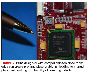
Components can be designed and spaced too close to each other or to the edge of the board (Figure 2).
Consequently, this error or oversight poses limitations for the
pick-and-place machine during placement. Parts must then be placed by
hand, creating reliability issues and likely leading to defects. An
alternative is to redesign the board, which involves a costly and
time-consuming re-fabrication.

Insofar
as component placement, a 0.004Ë pitch BGA, for example, requires
considerably tighter placement tolerance than a 0.007Ë or 0.008Ë pitch
BGA; thus, it demands more placement precision (and generally, more
expensive equipment). Even then, at 0.004Ë pitch, reliability and
repeatability can continue to be issues unless proper design measures
are taken.
Fabrication. First-article
is a critical step to verify virtually every aspect of PCB fabrication,
including hole size verification, cutouts, slots, and all physical and
mechanical dimension calculations. Eliminating defects at fabrication
also takes into account well-documented fabrication notes and an
extensive checklist of key factors. If any one or more factors are
overlooked or blatantly omitted, chances of defects increase.
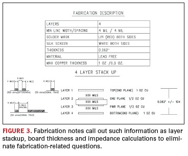
Here,
planning at the CAM stage calls for checking, double-checking, and even
triple- checking such factors as layer stackup structures’ thicknesses
and impedance control calculations to make sure they are precisely
correct and are within specified tolerances. The fabrication
description chart (Figure 3) shows a four-layer stackup, with all the key elements precisely described.

A
board’s innerlayers also can be a breeding ground for defects. Proper
design uses correct prepreg materials and core thicknesses to prevent
innerlayer registration problems. Similarly, applying correct board
surface finishes is of the utmost importance, especially for Pb-free
product. Where OEM cost is an issue, Pb-free HASL or ImAg may be the
right way to go for a Pb-free board. However, ImAg has a tendency for
corrosion.
In this case, pending corrosion would
not be immediately apparent. However, over time, it can begin to occur
in the field, creating one or more defects and subsequent product
failure. Therefore, a better choice could be ImAu. Again, experience
and know-how play into situations like this to make the right call.
Fabrication
notes also cover IPC class, according to the board that is going to be
built, such as Class 1, 2 or 3. Mistakes can occur if the fabrication
class is not properly called out in the fabrication notes. It’s also
important to document the percentage of warpage allowed. Defects can
arise from excessive warpage (bow and twist), improper etchback, plated
versus non-plated hole errors, and incorrect mechanical tolerances of
drill bits. Plus, drilled holes must have sufficient tolerances so they
become full holes without creating half moons or having stubs. These
and many other fabrication factors set the stage for defects.
It’s
also crucial to define the number of panel stackups for the drill and
routing stages. For example, in a six-board stack, specified drill and
routing tolerances may be achieved on boards 1, 2, 3 and 4, but not 5
and 6, due to mechanical drill limitations. To avoid this, the number
of panel stackups is defined as a process. Defining processes like this
within well-documented fabrication notes provides an extra measure of
assurance for eliminating defects. AOI can also be defined as a process
for inspecting innerlayers, especially for high-count layer boards
using extra thin prepregs.
Assembly. Multiple
factors can eliminate board defects at assembly stages. Like
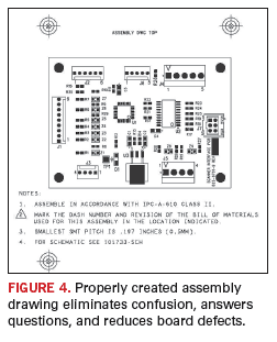
fabrication notes, there should be a comprehensive assembly drawing
detailing all the necessary assembly processes. For example, a process
can clearly spell out that all components, including BGAs, are to be
machine placed, as well as any rework or ECO callouts and the use of
any special process. Figure 4 shows an example of a
properly created assembly drawing, which can eliminate confusion,
answer questions, and reduce board defects.

Assembly
processes must be repeatable. The first article is important at the
assembly level as well, so technicians can check for polarities,
missing components and other key areas. Planning must be conducted to
determine and document the processes that need to be defined, the
machines needed, engineering change orders (ECOs) and use of special
equipment such as arbor press for press-fit connectors, AOI machines or
flying probe testers.
Documentation is important for
technicians in the field who need to read and decipher ECOs that
deviate from original build. Likewise, rework instructions, if any,
need to be clearly spelled out with solid quantitative data for
measurement and verification purposes.
At times,
instructions can be issued in an assembly drawing to avoid board
defects, which could be process-related issues. Also, depending on how
progressive an EMS provider is, post reflow inspection can be specified
as part of the process for all BGAs, CSPs and QFNs, as opposed to at QC
at the end of assembly. At this point, actions can be taken to avoid
board defects such as improper board reflow, poor orientation, wrong
thermal profile and improper flux activation, among other problems.
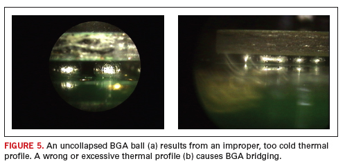
This
is important to eliminate defects. If the thermal profile is incorrect
and the board does not heat properly, the result will be cold solder
balls on the BGAs, CSPs or QFNs (Figure 5). If the thermal profile is too hot, bridging can result.

During
first article post-reflow inspection, while boards are going to reflow,
the process can be stopped; it can be changed and a set of one or two
boards as second articles can be run to correct the process. But if
some are not caught during the process, they are found at the end of it
when it can be too late. A shipment could be missed, or excessive
rework required, taking more time, resources and extra dollars.
Thus,
it is important for EMS providers to build QC steps within the
assembly/manufacturing process. It’s also important for OEMs to specify
process-related issues as part of the assembly drawing to avoid
defects. PCD&F
Zulki Khan is president and founder, NexLogic Technologies, Inc. (nexlogic.com); This email address is being protected from spambots. You need JavaScript enabled to view it..


