Increasing the thermal conductivity of the base materials improves thermal management in RF designs.
Looking
at the thermal issues which are impacting microwave design in today’s
marketplace, we see several drivers that will continue to require
better and more effective thermal management in the near future. Some
of these factors are relevant to all electronics packaging, such as
increased watt density on smaller package footprints, but others are of
particular importance to the microwave and RF industries. Among the
more important considerations for the microwave engineer are:
- Power density (Watts/square inch of PCB area) continues to increase
- Packaging is getting smaller & hotter (inherently increasing watt density still more)
- Tower mounted & outdoor electronics increase environmental exposure while requiring higher reliability
- Complex waveforms decrease amplifier efficiency, resulting in more energy lost to heat
- Higher temperatures reduce component reliability
- Dielectric constant of many materials varies significantly with temperature
When
the heat generated by an active device mounted on a PCB cannot be
dissipated, then the temperature of the device rises. With all the
drivers pointing toward more power and smaller board surface area, the
watt density becomes such that temperatures can easily exceed the
qualificated temperature for many of the individual components. Since
reliability of components follows a first order Arrhenius equation, a
10ËšC increases in temperature doubles failure rate, so even 1ËšC
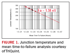
temperature increase matters. Figure 1 shows data
presented by Eli Reese of TriQuint, and presented at IWPC in November
2005, relating junction temperature to mean time-to-failure. The key to
reducing junction temperature is to increase the rate at which heat can
be removed from the device and from the working area of the PCB
immediately adjacent to the device.

The
cost of device failure can be significant since device failure accounts
for as much as 70 to 90% of equipment downtime, and in the case of
tower-mounted electronics, the cost can run several thousand dollars
for a simple repair that results in a short downtime. In bad weather
this can extend to a full day and cost as much as $25,000. Between
actual repair costs and potential lost revenue the implications of this
trend towards increased operating temperatures of PCBs is substantial.
The industry is looking seriously at solutions that can provide a
cost-effective way to mitigate the risk of failure.
Heat
is generated every time an active device is in operation. Heat itself
does not become a problem until there is an increase in temperature
above a critical point (typically 105 to 120ËšF). In simple terms, the
whole business of managing heat in a PCB assembly is about preventing
the junction temperature from getting high enough to “fry” the active
devices.
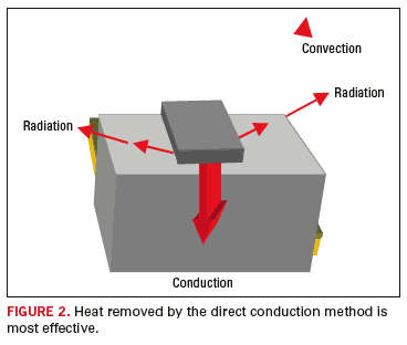
Heat is moved by one of three basic modes:
conduction, convection or radiation. In a PCB assembly all three are in
effect to one degree or another. The most effective is direct
conduction, where a warmer body is in direct contact with a cooler one,
and the heat moves from the hot to cold material (Figure 2).
The rate at which heat is carried from one to the other depends on the
thermal gradient, the coefficient of heat transfer of both materials,
the quality of the interface and to a lesser extent, the heat capacity
of the cooler body – that is its ability to absorb heat.

Convection
is the transfer of heat from a hot body to a cooler gas or liquid,
which carries the heat away. Convection may be aided by forcing the
cooling gas or liquid to flow past the warm body, removing the heat
more quickly. Radiation is the removal of heat from a body by the
emission of energy in the form of electromagnetic radiation, which may
be in the infrared (heat) or even visible (light) parts of the
spectrum, depending on the temperature of the radiating body.
Corollary
to consideration of the thermal conductivity (Tc) of laminate substrate
materials is also the fact that the heat transfer coefficient in the
perpendicular direction (through the PCB) is different from that in the
plane of the board. Unfortunately most modeling software assumes
isotropy, which may result in over or underestimation of the heat
removal.
Traditionally, a number of approaches have
been put forward to reduce temperature in PCBs by removal of heat from
active devices. The IWPC has been actively involved in assessment and
discussion of the various thermal management techniques, which include
the following:
- Laminated heavy metal backplanes (i.e. copper, aluminum, brass from 1 to 10 mm in thickness)
- Electrically and thermally conductive adhesion to plate (a good reference here is Ruwel)
- Thermal vias
- Thermal coins (a good example is the Merix E-Coin)
- Heat sinks, heat spreaders, heat risers (good references found at GrafTech)
- Thermally conductive adhesives, gap fillers, grease, etc.
- Active cooling – forced air, conditioned air
- Water cooled, vapor cooled, direct, indirect
While
all of these methods (note the predominance of the more efficient
conductive approach) are effective to varying degrees in the reduction
of junction temperatures, many of them have attributes that make them
less than ideal for use in microwave or RF circuit boards. Thermal vias
(a clusters of plated-through holes located beneath an active device)
are effective in removing heat because of the high thermal conductivity
of copper (370-400 W/m-K) but the plated through holes near the signal
traces can affect signal integrity, and a large number of plated
through holes can affect the mechanical strength of the PCB itself.
Heat
sinks and heat spreaders are heavy and expensive (a 3mm copper plate
can add as much as $25 to a single PCB) and devices such as thermal
coins that require cutouts result in increased fabrication complexity
and assembly costs. More sophisticated approaches such as forced
convection are costly, and may themselves be subject to risk of
electromechanical failure.
An attractive alternative
to total reliance on the traditional approaches of thermal management
is to build the underlying PCB with a dielectric material that is
inherently more thermally conductive. Conventional PCB materials having
a thermal conductivity of 0.2 to 0.25 W/m-K, and filled products range
from 0.4 to 0.6 W/m-K do not provide enough heat removal and heat
spreading capacity to do the job alone.
There are
new materials entering the market that have a 6.15 Dk and are suitable
for use as microwave substrate materials. These materials can provide
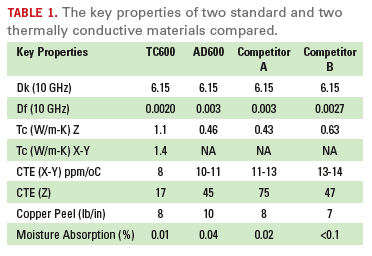
thermal conductivity (Tc) of 1.1 W/m-K perpendicular to the plane of
the board, and 1.4 W/m-K in-plane. This is more than double the best
thermal conductivity currently available in a standard microwave PCB
substrate materials, and high enough to allow designers to reduce
dependency on more costly approaches.
What benefit does increased thermal conductivity of microwave PCB substrates offer to the PCB designer?
- Component and solder joint reliability improvements would drive down warranty costs
- At constant heat rise, the improvement in heat transfer can be used to increase power handling by as much as 5-10%
Thermal stability of dielectric constant reduces dead bandwidth and
increases phase stability over the temperature range reducing design
limits and complexity
- It compliments all other alternative sources of thermal heat extraction at no additional cost
- Alternatively,
it potentially simplifies or lowers costs of other thermal solutions,
such as facilitating cast vs. machined heat sinks, and reduces in
copper plate thickness from 3mm to 1mm
The design objectives for the development of these thermally conductive materials included:
- Maintaining
the current material cost structure while improving dielectric loss
(loss tangent) and insertion loss to minimize heat generation in signal
transmission
- Increasing base laminate thermal conductivity (both perpendicular and in-plane) to reduce heat generation
- Maintaining laminate integrity in terms of key properties such as copper peel adhesion and low water absorption.
The
specific target products were to produced as 6.15 and 3.50 Dk materials
to meet the predominant industry demand for RF amplifier designs. Table 1 compares the key properties of two standard and two thermally enhanced conductive materials.

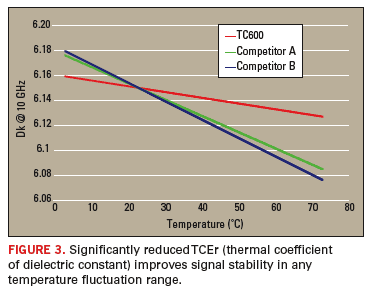
The
unique chemistry of the engineered laminate material includes a
significantly reduced TCEr (thermal coefficient of dielectric constant)
as seen in Figure 3. This translates into a more stable signal within any range of temperature fluctuation.

The improvements of this thermally enhanced material include:
- Temperature
insensitive materials help amplifier and antenna designers minimize
dead bandwidth, which is lost to dielectric constant drift as operating
temperature changes
- For antenna designs, a
significant shift in resonance frequency and bandwidth roll off at
specific frequencies, results in lower gain performance, and
- Thermal
stability is critical to phase sensitive devices, such as impedance
network transformers, utilized for matching networks of power
amplifiers
To illustrate the impact of
thermal conductivity both in the perpendicular direction, as indicated
by reduced temperatures measured at the active device, and in-plane, as
determined by the degree of heat spreading, a sample circuit based on
an RF power field effect transistor was developed and thermograms
obtained using thermally conductive laminate and a standard material
with a thermal conductivity of 0.46.
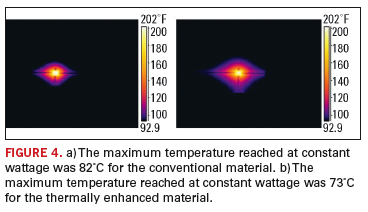
The results
were significant both in terms of the heat reduction at the top surface
and the spreading of the heat in the plane of the board. The resulting
thermograms dramatically illustrate the effect of increased thermal
conductivity. The maximum temperature reached at constant wattage was
82ËšC for the conventional material, 73ËšC for the thermally enhanced
material, a reduction of 10% and more importantly, a reduction of 9ËšC
that could be the difference between life and death for sensitive
junctions. (Figures 4a and 4b).

Summary
Traditional
laminates provide the greatest resistance (insulation) to heat
transfer. Increasing thermal conductivity of the base materials is a
new approach to thermal management in RF designs, with negligible
expected cost implications or impact on signal integrity. These
materials can provide improved component reliability as a result of
improved solder joint reliability. There is less work hardening, less
thermal expansion from lower retained heat and the materials have an
inherently lower CTE. Products designed with these materials will see
improved power handling, and these new thermally enhanced laminates
complement other more traditional thermal management tools. While
designed to meet the demands of RF circuits, these materials can also
be used as a replacement for traditional high performance FR-4
substrates where thermal management is a critical design constraint. PCD&F
Russ Hornung is technical marketing manager at Arlon; This email address is being protected from spambots. You need JavaScript enabled to view it.. Mike Smith is VP of marketing and R&D, also with Arlon, and can be reached at This email address is being protected from spambots. You need JavaScript enabled to view it.. Chet Guiles is an Arlon retiree and industry consultant, and can be reached at This email address is being protected from spambots. You need JavaScript enabled to view it..


