The use of full-wave electromagnetic modeling can simulate the
behavior of a high-speed differential backplane channel and advance the
system-level design process.
The operating frequency of high-speed copper backplane serial links
is expected to reach 10 Gbps in the next few years. At a 10 Gbps data
rate, the clock frequency is 5 GHz, equating to a period of 200 ps,
which results in a signal rise time in the range of 30 to 50 ps. This
rise time will influence the analog bandwidth and the highest
significant frequency component both for the measurement bandwidth and
the bandwidth of the channel model. To effectively design a serial link
(channel) to operate effectively at this bandwidth, accurate signal
integrity modeling is required.
A full wave
electromagnetic (EM) simulator is used to create models of the various
components (transmission lines, connectors, vias) on a high-speed
serial channel. These models are then verified with laboratory
measurements on a test vehicle containing backplane to daughtercard
links. The link contains two high-speed digital connectors, two modules
and a backplane. The frequency of operation is 0 to 10 GHz.
Three-dimensional EM models are created for all the link components.
The EM simulator provides S-parameters and time domain data, which can
later be compared to laboratory measurements.
Time
Domain Reflectometry (TDR) is used to measure the channel, and a
software tool provided by the TDR manufacturer is used. This tool
enhances the TDR capabilities, improves measurement accuracy and
creates S-parameter data from time domain measurements. This tool also
allows a designer to create SPICE models of the link components, based
on the measured data. The SPICE model results can then be verified by
comparing it to the measured data, and the final model assembly can be
used to predict the overall system response in the circuit simulation
environment.
In this paper, we will present the
major stages for modeling the gigabit backplane structure used in the
system-level design process. We will start from the description of the
interconnect structure followed by the full-wave EM simulation of the
design. The results of this simulation will be compared with the
measurement data of the prototype. Finally, a topological circuit model
created from the measurements will be used to predict data transmission
through the backplane in terms of an eye diagram.
Electromagnetic Modeling of the Channel
The
channel chosen for this analysis consists of two test modules, a
backplane and a high-speed connector. The connector is the 10-row FCI
AirMax connector. The commercial CST Studio Suite 2006BTM
software is used for the simulations of the channel, at a frequency
range of 0 to 10 GHz. CST Microwave Studio, a full-wave 3D EM modeler,
which uses the Finite Integration Technique (FIT), is used to model the
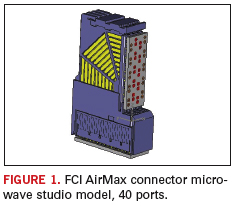
channel. The AirMax connector model in MWS is shown in FIGURE 1;
the 20 conductors on the inner two columns are simulated, and waveguide
ports are set up on both sides of the connectors, resulting in a 40
port simulation. The conductors on the outer two columns are terminated
in 50 ohms.

A broadband multiple port simulation is
best suited for the CST Microwave Studio (CST MWS) time domain solver,
which is based on a hexahedral Cartesian mesh and Perfect Boundary
Approximation (PBA) technique. The resultant Touchstone file has been
verified against empirical data to ensure the model accuracy.
The
modules consist of four layers, and the high-speed signals are located
on the top and bottom layers. The high-speed traces are 12 mils wide
and 1.8 in. long, with a characteristic impedance of 50 ohms. The
dielectric material on the modules is N4000-6 (FR4), with electrical
properties of εr=4.3 and loss tangent=0.019. The backplane is 20
layers, 230 mils thick. The channel routes are all on stripline layers,
and the backplane contains several layers of back drilling to minimize
the via stub effect. The channel traces on the backplane are 9 mils
wide, and Tx module to Rx module distance is 10 in. The dielectric
material on the backplane is N4000-13, with εr=3.9 and loss
tangent=0.012.
A CST MWS Frequency Domain (FD)
simulation is used to simulate the transmission lines on the modules
and backplane. The CST MWS FD solver employs a tetrahedral mesh and
accurately simulates dielectric high-frequency losses. The EM model
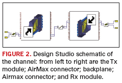
results of the members of the link (two modules, two connectors and
backplane), are combined in the CST Design Studio tool. Design Studio
is a circuit simulator that can extract S-parameters and time domain
data of individual concatenated blocks. See FIGURE 2 for a view of the Design Studio schematic for this channel.

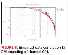
An S-parameter simulation is performed on the entire channel at 0 to 10 GHz. In FIGURE 3,
the resultant S31 (through) of the channel is illustrated and compares
this to the measured data. A good correlation can be observed across
the entire frequency range.

Measurement Methodology
Once
the prototype is manufactured, its performance must be verified as a
part of the overall system, and this can be efficiently done in the
SPICE circuit simulation environment. For this purpose, the
measurement-based topological modeling methodology is the most feasible
candidate. Once the model is generated, a designer can look at the
different parts of the circuit model and see how they will affect the
final data transmission. In the following subsection, we will briefly
describe the measurement-based topological modeling methodology applied
for the same gigabit backplane structure.
In general,
measurement-based modeling strategy follows four major steps: measure,
model, verify and simulate. Although the measurements can be done in
time or frequency domains (converted to time), the preference is given
to the time-domain measurements because they allow for better
resolution for the same measurement bandwidth. The modeling is then
performed on time domain voltage or impedance data by applying
different strategies for various features of the gigabit backplane. For
example, relatively short and lossless discontinuities, such as
connectors and vias, can be easily modeled using lumped circuit
elements or adding short pieces to the ideal transmission lines,
whereas long traces can be modeled using a uniform lossy transmission
line model. After the model is generated, it is imperative to compare
it with the measurements and adjust its components to obtain the best
possible correlation. The final step is to simulate different data
patterns to see if the interconnect will perform as expected.
Step 1: Time-Domain Measurements
To
measure the backplane structure, a Tektronix CSA8200 sampling
oscilloscope with the IConnect software from the same company was used.
The time domain sampling oscilloscope generates a high-speed time
domain step that propagates through the interconnect structure. The
reflected and transmitted step response can be converted to the
frequency domain to obtain S-parameter data such as return and
insertion losses.
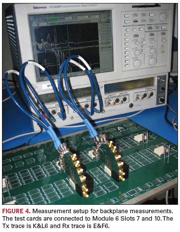
The measurement setup used in the analysis is shown in FIGURE 4.
It consists of the sampling oscilloscope with two high bandwidth (20
GHz) sampling modules connected via SMA cables to the test cards of the
backplane. Time domain reflectometry measurements allow viewing of the
interconnect characteristics in time. The measured data can be
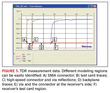
displayed as impedance, reflection coefficient or voltage waveforms. FIGURE 5
shows the result of these time-domain measurements. Different regions
of the backplane structure can be easily identified from the time
domain measurements by disconnecting the test cards from the measured
backplane structure and observing time domain reflections from the
opens at different points.


When a signal enters the
backplane structure, it first sees the discontinuity due to the SMA
connector of the test card; this is point A in Figure 5. The SMA
connector is then followed by the test card’s trace labeled as the
region B in the figure. After that, the signal sees a
test-card-to-backplane connector and the via-to-trace discontinuities
are labeled as the region C. Then the signal propagates through
differential traces of the backplane structure (region D) finally
approaching the receiver’s test card side, where regions E and F
indicate the via-connector and test-card traces, respectively.
Step 2: Modeling of Reflections and Losses
After
identifying the different regions, a designer can start performing
modeling. The reflections from the SMAs, high-speed connectors and vias
can be modeled using lumped elements or pieces of ideal transmission
lines, while the traces have to be modeled with lossy transmission
lines. The next figures illustrate the general modeling procedure to
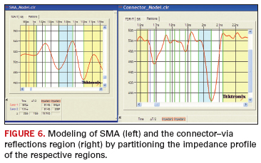
model the backplane structure shown in Figure 1. FIGURE 6
shows the impedance profile-based modeling of the reflections from the
SMA and high-speed connector regions. To model the structure, the
impedance profile is simply subdivided into the different regions and
ideal transmission lines are assigned for each region.

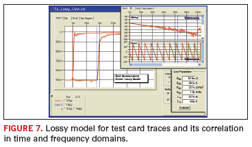
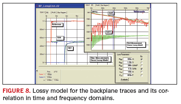
The
test card and backplane traces are relatively long structures that
exhibit lossy behavior and have to be modeled with lossy transmission
lines. FIGURE 7 and FIGURE 8 show
the lossy models (and their correlation with the measurements) created
for the test card and backplane traces respectively. Note that the test
card model was obtained from TDR data only, while the backplane’s
losses were obtained from TDR and TDT measurement data.


Step 3: Verification of Model’s Performance
When
individual components for the backplane model assembly are generated,
an engineer can assemble the model and verify its performance with the
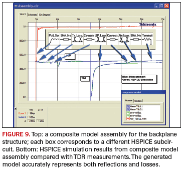
measurements when the same step is applied to the generated model. When
all modeling pieces that correspond to reflections and losses for the
channel are assembled together, each of the individual components can
be fine tuned to archive the desired accuracy in terms of reflected and
transmitted data. The general model topology and time domain
correlation are shown in FIGURE 9.

Step 4: Simulation of Data Transmission
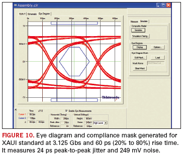
Once
an accurate model is generated, it can be used to predict real signal
propagation through the interconnect structure. Different data patterns
can be easily synthesized with the software and their response can be
plotted in a form of an eye diagram. FIGURE 10 shows
the channel model’s synthesized eye diagram generated for XAUI data
rates. It measures 24 ps peak-to-peak jitter and 249 mV noise at 3.125
Gbs and 60 ps (20% to 80%) rise time.

Summary
We
have shown the feasibility of using full-wave electromagnetic modeling
to simulate the behavior of a high-speed differential backplane
channel. The simulated results match well with empirical data. The
measurement technique described consists of taking TDR measurements and
using software to create S-parameter data and an accurate model of the
channel. PCD&F
Ed note: This paper was previously presented at PCB Design Conference East in Durham, NC, October 2007.
Acknowledgements
Many
thanks go to Martin Schauer and Antonio Ciccomancini at CST for the
valuable feedback provided on the modeling of this channel. We’d also
like to acknowledge the assistance of Dana Bergey and Jonathan Buck,
with FCI, who provided the test vehicles used in this experiment and
the model file for the AirMax connector.
Eugene Mayevskiy is an applications engineer at Tektronix; This email address is being protected from spambots. You need JavaScript enabled to view it.. Fabrizio Zanella is the support manager at CST of America; This email address is being protected from spambots. You need JavaScript enabled to view it..
REFERENCES
1.
J. S. Pak, J. Kim et al., “Coupling of Through Hole Signal Via to
Power/Ground Resonance and Excitation of Edge Radiation in Multi-layer
PCB, IEEE Int. Electromagnetic Compatibility Symposium, Boston, MA,
Aug. 2003, pp. 231–235.
2. CST Studio Suite 2006, cst.com
3. A. Ciccomancini, F. Zanella., “Broadband Signal Integrity
Characterization of a High Speed Differential Backplane Pair”, IEEE
International Symposimum on Electromagnetic Compatibility, Portland,
OR, Aug. 2006, pp. 24-28.
4. R. Kollipara, B. Chia, F. Lambrecht, C. Yuan et al, “Practical
Design Considerations for 10 to 25 Gbs Copper Backplane Serial Links”,
DesignCon 2006.


