BGA miniaturization amplifies the design challenge of balancing
high-performance signal integrity with fabrication cost reduction.
This is the first in a series of articles that will run in Printed Circuit Design & Fab
about BGA routing methods. My focus will be on design techniques using
common and advanced technologies for large BGAs to provide efficient
fanouts, dense routing and layer reduction.
These
articles are intended for PCB designers, exploring the impact of dense
BGAs with high pin-count, and to provide solutions for these inherent
design challenges on PCB design. There are volumes of information about
BGA package technology that look at the device from all aspects –
materials, thermal characteristics, assembly methods, reliability, and
electrical performance – yet little guidance is available regarding
effective PCB design methods.
BGA density and pin
count continues to increase, and our ability to effectively design with
these devices has not kept pace. Fortunately, significant advancements
in PCB fabrication technology have enabled further miniaturization in
the manufacturing process. These improvements, along with new software
and methods specifically designed for BGAs, provide the means for
successful design using these devices.
The
increasing pin-count and decreasing pin-pitch of BGAs amplifies already
difficult design problems. Maintaining signal integrity at high
performance levels while reducing fabrication costs are the two most
important, but conflicting, requirements. Reducing crosstalk is
generally accomplished by increasing the space between conductors,
which can increase layer count, plus routing through dense BGA pin and
via arrays requires smaller design rules. Increasing layers while
minimizing features contribute significantly to increased board cost.
This is nothing new, yet further miniaturization of BGA packages will
make it even more difficulty in maintaining performance and cost goals.
PCB
designers who are working with large pin-count BGAs (over 1500 pins)
often claim that the breakout of the device is the greatest contributor
to increased number of PCB layers. An efficient breakout solution will
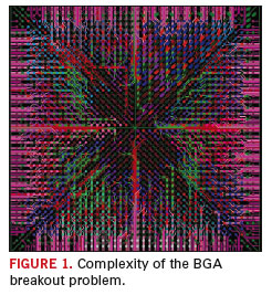
provide a foundation for layer reduction. I use the term “BGA breakout”
to describe a fanout design solution that routes escape traces from
fanouts to the perimeter of the device prior to general routing of the
PCB. Figure 1 illustrates the complexity of the BGA breakout problem.

Why
the need for breakouts? The answer is simple. If the BGA device has a
large number of pins in a dense array, the only way to minimize board
layers is to utilize available space inside the component area by
incorporating patterns for fanouts and breakout traces. Routing such a
device without effective patterns will certainly waste space and
require more layers.
Not all BGAs present a routing
challenge. Medium and low pin-count devices (less than 800 pins), even
with a pin-pitch of less than 0.8 mm, do not present a significant
breakout problem and are usually routed without a breakout method. This
means the pins are generally accessible and can be routed without using
an excessive number of layers.
The high pin-count
devices with a pin-pitch of 1 mm or less require a strategy for getting
traces out of the array. Without a breakout strategy, layer count will
be excessive, thus affecting the fabrication cost and reliability of
the PCB.
Additional factors complicate the breakout
process. To attain performance and cost goals, there are many variables
that must be defined and managed properly in concert with each other.
Layer
stackup. Early in the design process, the layer stackup will be
defined. If the board has large, dense BGAs, a High Density
Interconnect (HDI) with a laminated core and buildup layers may be
required. There are many different material and process options. Cost
and reliability are usually the primary factors in determining the
stackup, and there may be a tradeoff between layer count and the
fabrication process in order to reach your goals.
Via
models. Within the context of any given layer stackup, you have many
options regarding via models. The decision on which type of via to use
(through-hole, laminated blind and buried, or HDI micro vias) will
likely be driven by the density of the board and the BGA packages.
There are many options regarding stacking and vias inside pads that
effect cost. In addition to this, board fabricators tend to focus on a
limited set of manufacturing processes, making the choice of vendor
dependent upon the technology you desire. From the design point of
view, choosing the appropriate via models directly impacts the
routeability of the board.
Design rules. PCB
fabricators continue to find methods that allow further miniaturization
and increased reliability. Design rules must balance the tradeoffs of
cost, signal integrity and routeability.
Signal
integrity. Although the fabricators continue to improve their processes
and produce reliable boards with increasingly smaller features and
clearances, maintaining signal integrity at high performance levels
usually requires greater spacing between critical nets, especially when
attempting to eliminate crosstalk effects at higher speeds. This
conflict is exacerbated with high pin-count and dense BGAs. Choosing
appropriate layer stackups and via models will not only improve
routeability, but signal integrity as well.
Power
Integrity. Managing power distribution effectively for large pincount
BGAs is a challenge and is significantly impacted by the layer stackup.
There are methods that can minimize the number decoupling capacitors
required, thereby increasing the space available for signal routing.
Because of the high number of variables with any PCB design, it is not
possible to have a single BGA breakout solution for all. It is possible
however, to develop solutions within a reasonable set of variables.
PCD&F
Charles Pfeil is a product marketing
director for Mentor Graphics, Systems Design Division. He was the
original product architect for Expedition PCB and an inventor of
XtremePCB; This email address is being protected from spambots. You need JavaScript enabled to view it..


