To control emissions, high-speed signals should not be routed near the edge of the ground-reference plane.
It
is often difficult to route all the required traces on a PCB. There is
a constant goal to keep costs at a minimum and so the number of layers
available for routing is very limited. This can force designers to
route traces too close to the edge of the PCB. Routing too close to the
edge of the PCB can increase emissions from the edge of the
ground-reference plane. Controlling these emissions is simply a matter
of not routing high-speed signals near the edge of the ground-reference
plane.
Amplitude of Current Along the Edge of the PCB Ground-Reference Plane
In
the case of both microstrip and stripline, the majority of return
current will flow in the plane nearest to the trace. However, some of
the return current will spread away from the trace to find the path of
least impedance. As the trace is routed further from the edge of the
plane, less current is along that edge. However, it can still be
significant for EMI/EMC purposes even when too low for signal integrity
concerns.
Equation 1 gives the formula to find the
current along the edge of a ground-reference plane for a microstrip
transmission line1. The currents on each reference plane for a
symmetrical strip line are simply one-half of those in Equation 1.

where:
Isignal = the current amplitude (in linear scale) for each harmonic of the current waveform.
wg = the width of the ground-reference plane (set to 1000 mils always)
d = the distance from the trace to the edge of the ground-reference plane in mils
h = the height between the trace and the ground-reference plane in mils
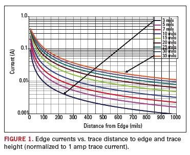
Equation 1 is plotted in Figure 1
for a microstrip with a variety of different trace heights and
distances to the edge of the ground-reference plane. The amplitude of
the current along the edge of the ground-reference plane decreases as
the distance between the trace and the edge increases. Also, when the
trace height is further from the reference plane, the current along the
edge is higher.

Impact with Real-World Signals
Let’s
consider a typical frequency spectrum for a clock signal’s current. In
this case, we’ll assume the current waveform follows the voltage
waveform, as in the case of a resistive termination for this clock net.
Of course, if a non-resistive termination is used, the frequency
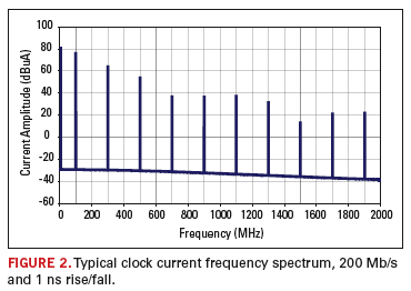
spectrum will be different. Figure 2 shows the frequency spectrum for a 200 Mb/s square wave with a 1 ns rise and fall time.

For
this case, the 5th harmonic occurs at 900 MHz, and its amplitude is
approximately 40 dBuA (100 microamps). If the trace is 50 mils from the
board edge, and the trace height is 10 mils from the plane, then the
edge current will be expected to be approximately 60% of the trace
current, or 60 microamps. However, if the trace is moved to 0.5Ë from
the edge, the edge current falls to 6% of the trace current, or 6
microamps.
How Much is Too Much?
It
is very difficult to calculate the expected far field radiated
emissions without knowing specific information about PCB, including its
size, shielding metal enclosures, etc. However we can consider that the
edge of the reference plane will be an efficient radiator when it is
one-half a wavelength long. Equation 2 shows the
formula to find the wavelength. For example, at the 900 MHz the
wavelength is only 33 cm and a half wavelength is 16.5 cm
(approximately 5 inches). Clearly, many PCBs will be large enough to be
efficient radiators at these frequencies.

where:
λ = wavelength
c = speed of light (300e8 m/s)
f = frequency
εr = relative dielectric constant
A
general rule-of-thumb is that a few microamps of noise current on an
unshielded and efficient wire antenna can cause emissions that will be
over the commercial EMC emissions limits. So depending on the amount of
shielding, emissions from edge currents may be important.
Summary
The
distance between the trace and the edge of the ground-reference plane
is important for EMI/EMC. Most of the return current will be below the
trace, but some of this return current will spread out over the
reference plane. If the trace is too close to the edge, then emissions
will be higher than if the trace is further away from the edge. These
emissions can easily be higher than allowed by commercial emissions
standards.
This does not mean that the routing
channels near the edge of the board may not be used and must be left
blank. Most boards need every routing channel possible. Use these
routing channels near the edge of the reference plane for low speed
signals and keep the high-speed clock, data, address, etc. signals away
from the edge of the reference plane. PCD&F
REFERENCES
1.
M.Y. Koledintseva, J. Drewniak, T. Van Doren, D. Pommerenke, M.
Cocchini, D. Hockanson, “Method of Edge Currents for calculating mutual
external inductance in a microstrip structure,” Accepted for
publication Progress in Electromagnetic Research (PIER), Feb 2008.
Dr. Bruce Archambeault is an IBM Distinguished Engineer and IEEE Fellow; This email address is being protected from spambots. You need JavaScript enabled to view it..


