The merger of micro and nano, chemical, and other sensors with micro- and nano-electronics could mean disruption ahead.
Consumer and professional electronics are constantly evolving,
driven by the need for lower cost, higher speed, more memory, better
displays and smaller form factors. This, combined with wireless
connectivity, new functionality and longer battery life in handheld
devices, are forcing traditional methods and materials to a breaking
point.
Electronics system miniaturization for
mobile computing, communication and sensing will drive a new generation
of low-cost packaging technologies over the next decade.
Multifunctional integration, ultra small form factor and low cost will
be the defining characteristics of next-generation packaging. This new
packaging technology will interface with integrated or embedded active
and passive components, cooling structures and advanced interconnect
structures in ultra-thin silicon and organic type substrate platforms.
Chip and package co-design and considerable integration of digital, RF,
optical, sensing and biological functions in 2-D and 3-D architectures
will be realized. These technologies will need advanced materials with
enhanced electrical, thermal and thermo-mechanical properties, and
advanced manufacturing processes.
The 2007 iNEMI
Roadmap1 identified a number of key areas where rapid development or
discontinuous change may be required to meet these needs. The iNEMI
research priorities recommended three areas for action:
Innovative
packaging for gigafunctional system-in-package (SiP). Traditional
interconnections of surface-mounted discretes are being changed to
ultra-fine-pitch interconnections connecting embedded ultra-thin film
components on ultra-thin silicon and organic type substrates. The
package integration will evolve into system integration, leveraging the
system-on-chip, wafer-level packaging and embedded passives and actives
on organic substrate technologies. Convergent micro- and nano-systems
will have not only digital and portable wireless electronics, but also
bioelectronic functions. These electronics and bioelectronics devices,
advanced interconnects, batteries, thermal solutions and other user
interfaces such as connectors and cables can lead to multifunctional
systems in the short term and more integrated gigafunctional systems in
the long run. This SiP concept integrates disparate technologies to
achieve multiple system functions in a single package, while providing
an ultra-small form factor.
Materials and
reliability. Materials must continue to keep pace with packaging
technologies to meet the major manufacturing requirements of low cost
through increased modularity, integration for smaller size, and higher
bandwidth for more functionality. In addition to these product-specific
attributes, there are general requirements for environmentally
friendly materials systems (e.g., bio-based polymers) that use
low-energy processes. While traditional technologies have focused on
materials systems for electronic performance, future materials
requirements will need to embrace optical, mechanical, and chemical
performance for electro-optical, microelectromechanical systems (MEMS),
chemical and biosensor systems, respectively. Advanced nanocomposite
and nanoengineered filler materials incorporating property improvements
not available with micron-sized fillers offer the promise to meet some
of these enhanced performance requirements. These property improvements
include low CTE with high toughness, high electrical conductivity with
low thermal conductivity (high ZT), and high compliance with high
current carrying capability.
Several technologies
may impact material packaging trends in the near and mid-term. In
addition to shrinking the IC with higher density PWBs, embedded
passives (resistors, capacitors and inductors) and embedded active
devices lead the drive toward small size. A key goal is higher
dielectric constant materials to produce embedded passives for
de-coupling capacitors. Innovative designs and special types of organic
substrate materials could also give high Q inductors. Solder systems
have migrated to higher reflow temperature ranges due to the drive for
Pb-free solder systems, placing severe thermal loads on the existing
material systems as they traverse the reflow zones.
Underfill
processes, which improve mechanical performance of parts soldered to
the PWB, increase assembly time, leading to increased assembly cost. To
reduce the delays associated with underfill assembly for ICs or
semiconductor packages, underfill materials will be pre-bonded or will
be thin films applied to the PWB by pick-and-place machines. As
alternatives to solder attach, conductive adhesives (liquid or thin
film) will become more common for low-temperature processing and
fine-pitch assembly, assuming they can satisfy the bandwidth
requirements for higher performance systems. Self-assembly methods are
also evolving to address the challenging assembly needs of ultra-thin
small dies in large volume. A number of innovative options are being
pursued in the development of reliable fine pitch interconnect
materials and assembly processes.
Printed electronics
will develop in the longer term. Produced on flexible substrates and
using conductive, dielectric, semiconductor, and light emissive inks,
these materials have the potential to transform segments of the
electronics industry. Innovations will be needed for existing material
systems to address ink sensitivity to humidity, oxygen and light.
Sensors.
The rapid acquisition and processing of data from any type of available
sensor such as mechanical, acoustic, thermal, chemical, seismic,
environmental and biological will become integrated into many areas of
daily life. Intelligent integrated sensing and control systems are
migrating from islands of automation to interconnected solutions, and
subsequently to intelligent self-managing highly scalable systems
(i.e., autonomous active control and monitoring systems). This
evolution requires coordination and leverage across multiple
technologies such as sensing, monitoring, control and communications.
Sensor technologies, management tools and gateways will play a central
role in enabling the higher level of integration needed in the
development of these new intelligent sensing and control systems.
Beyond these sensor fusion elements, architectural considerations are
required to coordinate this evolution to address scalability issues
such as performance, global universal object identification, system
management and security. These large sensor networks will require
unique solutions in the acquisition, transmission and processing of the
extensive amount of information gathered for robust networks.
Sensor
network development involves deployment of the sensors and the network
elements to collect and transmit data for analysis and action. These
sensors and their local processors and communication function may take
the form of a SiP. An increasing number of these sensors are realized
using micromachining technologies in the form of MEMS devices. Thus, a
packaging base is needed that can support mechanical, acoustical,
thermal, chemical, seismic, environmental and biological sensors, as
well as optical and RF communications.
It is
important to identify the correct number of nodes and sensors needed to
get the most accurate information at the lowest possible cost. The
networks are likely to have a multiplicity of sensors, and it’s vital
to determine the number and placement of the sensors within the
“network field.” Redundant sensors provide more accurate information;
however, with the large amount of data that can be collected from
deployed sensors, it is important to identify how and where to fuse the
data.
Self-organizing wireless nodes will form the
basis for new networks. These networks will require localized signal
processing capability. Ultra-low-power IC designs, mixed-signal
module/SiP designs, sensor packaging and integration technologies will
generate many new innovation options. Data from the network of sensors
will be transmitted to gateway devices with the capability of
processing and determining the relevance of data. The gateway devices
will store, analyze, and relay data to where it is needed. The
transmitted data would then be used to make appropriate decisions on
what actions need to be taken.
Nanotechnology: Strong Implications
Nanotechnology
has the potential to address these three emerging issues, particularly,
the construction of new materials based on nanoparticals. Most
nanotechnology applications are still in the pre-commercial stage, and
will need development not only of products but also of modeling
techniques and metrologies. Products are being developed and
commercialized in large and small companies with strong nanotechnology
initiatives.
Nanotechnology in its various forms
has strong implications for the competitiveness of the electronics
industry. The combination of significant nanotechnology R&D with
technology transfer obviously represents business opportunities.
Nanoscale materials are already well represented in the electronics
industry today, including nanocomposites and nanostructured packaging
materials, sub-100 nm IC structures, and thin-film giant
magneto-resistive (GMR) read heads for high-density disk drives.
Nanotechnology advances will contribute a number of products and
processes that could be especially relevant to electronic processes and
products, ranging from the extremely long range and innovative to the
short range and drop-in, including:
- Quantum computing using “peapod structures” based on carbon nanotubes (CNT) or Bose-Einstein atomic clusters (long term).
- DNA strand self-assembly of electronic structures (long term).
- Transistors based on CNT or GMR layered structures (long term).
- Mixed nano and MEMS sensor technology (medium term).
- Plasma display technology based on CNT emitters (medium term).
- Advanced
fillers for nanocomposites and nanoengineered materials with property
improvements not possible with micron fillers, such as low CTE with
high toughness, high electrical conductivity with low thermal
conductivity (high ZT), and high compliance with high current carrying
capability (short term).
- Nano-enabled solders and printable electronic structures using nano-sized metals, particularly silver and copper (short term).
Commercialization
of nanotechnology products and eventual replacement of existing systems
will depend on cost and performance, as well as the dynamics of new
market creation. The iNEMI Roadmap process will continue to monitor
advances in nanotechnologies and assess how these advances meet the
electronics industry’s R&D needs.
Conclusions
As
we move beyond the digital convergence of electronics products, we
anticipate the merger of micro and nano, chemical, mechanical and
biological sensors with micro- and nano-electronics for disruptive
innovations in many areas. In some cases, the disruptive technologies
may also find application by being embedded in conventional product
embodiments. As an example, nanoparticle fillers may enhance select
properties of existing polymeric materials. These applications will
likely result in new opportunities to extend the life of current
materials and manufacturing infrastructure, enabling them to deliver
enhanced device or component functionality. Breakthroughs may take the
form of disruptive technologies that supplant existing technologies.
Examples of these are quantum computing systems, molecular electronics
and spintronics replacing CMOS semiconductor technology. Others may be
radically new applications, such as sensor and drug delivery systems
that detect emerging disease in the body or treat existing conditions.

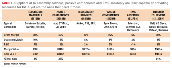
The
electronics industry restructuring over the past decade from vertically
integrated OEMs to a multi-firm supply chain has resulted in a
disparity in R&D needs versus available resources. Critical R&D
needs exist in the middle part of the supply chain (IC assembly
services, passive components, EMS assembly) (Table 1),
and yet these are the firms least capable of providing the resources. A
partial solution has been the development of vertical teams to develop
critical new technology while sharing costs. The entire industrial
supply chain, universities, research institutions and governments need
to not only create innovative technologies, but also creative solutions
for financing the R&D base that generates these innovations. This
must be done in a way that deals with IP in a distributed fashion
(rather than the traditional single-company approach) so that ROI for
the R&D investments are fairly apportioned, thus encouraging
sustainable innovation. PCD&F
Au. note: This article is
based on information from the 2007 iNEMI Research Priorities, available
at
http://thor.inemi.org/webdownload/RI/iNEMI_2007_Research_Priorities.pdf.
References
1. 2007 iNEMI Roadmap, March 2007.
Alan
Rae is director of research at iNEMI (inemi.org) and vice president of
innovation at NanoDynamics Inc. (nanodynamics.com);
This email address is being protected from spambots. You need JavaScript enabled to view it.. Robert C. Pfahl is vice president of operations
and Charles Richardson is director of roadmapping at iNEMI.


