Understanding the critical process steps in design, fabrication and
assembly can increase the robustness of the PTH and improve reliability.
PCB real estate, along with components, vias, and annular ring sizes
are shrinking dramatically. Five or 10 years ago, a via hole of 15 to
20 mils with a 5 to 10 mil annular ring was the norm. Now, via sizes
ranging from 7 mils down to 4 mils on highly complex boards are
increasingly more common. As through-hole size (via) shrinks, so does
the annular ring, posing major challenges to fabrication and assembly
manufacturers in the process.
In earlier PCB
generations, two to three mils of play (or wander) within a 10 mil hole
was common. Currently, precision laser drilling allows about 0.5 mil
wander, (sometimes less) as smaller drills have reduced via size to 4
or 5 mils. To illustrate, this means that one mil of wander represents
25% of the hole size when a four mil via is created.
Consequently,
tighter fabrication and assembly controls and tolerances,
state-of-the-art equipment and trained technicians must be utilized at
design, fabrication and assembly to assure high plated through-hole
(PTH) reliability. Laser drilling equipment must be up-to-date, highly
precise and accurate to ensure that vias and annular rings remain
intact as a PCB undergoes the multiple heat and reflow cycles during
the different phases of fabrication and assembly.
Sufficient
clearance is necessary to avoid creating break out on internal layers.
This condition is typically caused by miscalculations of drill size,
pad size, incorrect annular ring size or over-etching at fabrication,
resulting in weak or broken continuity.
Lead-free
design, fabrication, and assembly are especially vulnerable areas
requiring careful attention to assure PTH reliability. Experienced EMS
providers fully understand that proper focus must be placed on
selecting the correct PCB material, ensuring proper thermal profile
characteristics, and choosing the right flux as part of assembly
precautions in order to insure long term PTH reliability.
Currently,
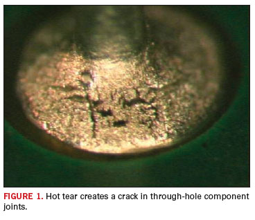
the lead-free assembly industry is experiencing an anomaly called “hot
tear,” which occurs with the use of SAC305 lead-free solder. As shown
in Figure 1, hot tear is a crack created in a through-hole component joint. SAC305 manufacturers are now investigating this problem.

With
lead-free projects, PTH reliability is also dependent upon the right
choice of flux at PCB assembly levels. Contract manufacturers (CMs) are
now dealing with a very narrow window of flux activity at a
considerably higher temperature levels. At these higher temperatures,
error tolerances are greatly reduced. Without the correct solder and
flux composition and proper thermal profile, PTH reliability is
severely jeopardized.
At Design
A
major function in DfM of the PCB is to determine accurate calculations
for through-holes and plated slots. These calculations apply to
determining via diameter in relation to annular ring size; another is
setting correct via spacing and consistently maintaining that spacing
for good signal integrity.
Accurately calculating
drill hole and annular ring sizes is critical. A larger hole diameter
requires a larger annular ring. Miscalculation in annular ring design
creates long-term reliability issues, especially at rework levels.
Experienced and disciplined designers refer to IPC610D and IPC221A
charts to obtain PTH and annular ring definitions as a basis for making
precise calculations.
The designer must also
carefully select the proper type of copper foil when designing a PCB.
Choices for copper foil are typically one-half, one, or two ounces.
When one-ounce copper foil is used, each square inch of the board will
be layered with one ounce of copper. However, in an analog PCB
application designed for higher current, a two ounce copper foil may be
required to insure the capacity for proper current flow. The choice of
the correct internal copper foil is an important consideration in PCB
long-term, reliability.
The copper deposited on the
hole wall through the plating process is also critical in the PTH
reliability equation. If insufficient copper is deposited on the via
wall long-term reliability can be affected. The problems created by
thin copper can include fractures or cracks in the barrel of the via,
leading to poor solder joints and intermittent or broken continuity in
the current flow. Recently the IPC reduced it’s the PTH thickness
requirement to a minimum of 0.8 mils. In some cases this may not be
sufficient copper for a particular design. If designers require more
copper in the PTH they will need to specify it on the drawing or the
fabricator can use the IPC guideline.
Connectors
and sockets require special design attention. Performing the right PTH
calculations are particularly critical because connectors and sockets
demand greater PTH precision, especially for press fit connectors. If
drill sizes and annular rings are calculated poorly, there is the
possibility of creating a through-hole that is too small to accept the
connector. And while it may be possible to maneuver a component lead
into a too-small plated-through hole, such actions often increase the
probability of cracked vias in the middle of the wall, creating an
unreliable connection. This problem can either immediately surface
during test, or become a latent or intermittent defect, causing
reliability issues for products in the field.
Reliability
becomes a major issue when via-in-pad technology is used. In some
manufacturing schemes, via-in-pad uses different materials and
processes than are used in conventional through-hole via. In some
cases, a conductive material such as epoxy or silver is used to fill
the via. For via-in-pad, a PCB fabricator must fully understand how
these materials will differ from the conventional via creation to
maintain the board within its own specific tolerances. This is a
challenge because the technology is still new, there are few
fabricators that have the necessary trained staff, experience, and
equipment to provide the high level of PTH reliability required today
from this technology type.
Plated through holes
using SMA connectors in high-speed designs require simulation modeling
also known as via modeling. This software assures there are no
reflections or discontinuities along along the electrical signal paths
to assure certain transition points are smooth. This is especially
important when there is a cable or connector used in the board.
Therefore, the optimal design requires that through hole components and
vias are designed with proper transition points, eliminating
reflections, discontinuities, or sudden changes in signal impedance
requirements.
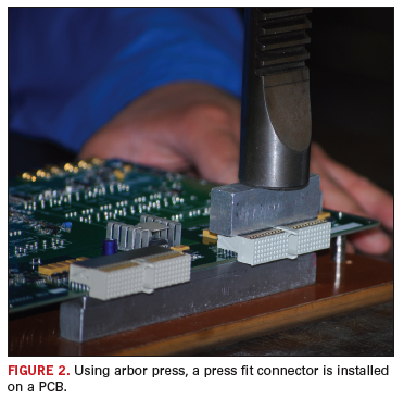
Rework cycles should also be considered
at PTH design. This is especially critical to press fit connector
reliability, as the connector will not tolerate warp or movement of the
board (see Figure 2) and is more prone to defects
during rework cycles. Extremely accurate PTH design is required for
these connectors, as after a mistake in the PTH process is made,
reworking a press-fit connection is extremely difficult. If the via is
too small, the connector won’t insert into the board; if too big, an
intermittent connection is created.

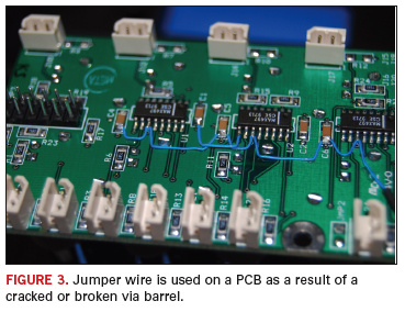
One of the few rework options involves cutting and adding jumpers. As shown in Figure 3,
an incorrect PTH calculation resulted in a too-small PTH. The via broke
off the board, and an unsightly jumper wire is used to recreate the
connection. Besides the aesthetic considerations, this repair method
lacks the level of reliability of a properly designed via.

At Fabrication
When
considering drill and pad sizes, a ± 3 mils tolerance is typical for
vias up to a 10 mil size. Some are tighter, where tolerances could be
+3 and -0 for a 7 mil or smaller sized via. There are specific
guidelines for drill hole and pad sizes. For instance, a 10 mil drilled
hole must have at least a 22 mil annular ring, allowing at least a 6
mil annular ring on each side. When space permits, a larger annual
ring, such as 26 to 30 mil would be preferable, to create a more solid
pad joint able to withstand several component extractions and
placements, as well as being able to undergo multiple reflow cycles
without incurring problems.
Aspect ratio, which
refers to the comparison of board thickness to the smallest via created
on that board, must also be carefully reviewed, as it plays an
important role in PTH reliability. The greater the aspect ratio, the
more difficult it is to fabricate the board and to assure that it’s
plated through holes will maintain reliability throughout the product
life. A 10:1 or 12:1 aspect ratio is standard, but there are now 30:1
ratio PCBs constructed for specialized applications. This 30:1 aspect
ratio board requires more precise pad-to-hole ratio calculations for
PTH reliability. It’s important to maintain robust drill sizes and
annular rings for high aspect-ratio boards to avoid half-moons and
breakouts.
The different board fabrication cycles
need to be followed and precisely implemented. This includes a number
of precise process sequences that must be at specific temperatures for
defined periods of time. There is always the possibility that a quick
turn order will have a few corners cut. The OEM must be sure that the
PCB fabricator doesn’t shorten the bake cycles in order to meet tight
shipment schedules. This can severely compromise long-term product
reliability. Such shortcuts could result in numerous problems, from
insufficient material cure and moisture absorption to incomplete
stabilization of the processing materials.
In
addition, if preventative maintenance is not regularly conducted on the
various chemistries used plate and process the PCBs, they it may become
contaminated or may stop performing as required. This contamination, as
in the case of a contaminated copper electroplating bath, can cause
vias to be more susceptible to cracking during the reflow cycles in the
assembly stage.
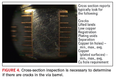
A cross-sectional inspection and
analysis, as well as other relevant testing, are often required to
pinpoint hairline cracks in the via’s barrel (Figure 4).
These defects may not be readily apparent and may pass a non-stressed
electrical test at the PCB fabrication facility and through the final
quality control without notice.

Two
tests are used to further insure PTH reliability. The first is a PTH
Life Curve; the second is a Current Induced Thermal Cycle Test (CITC).
The PTH Life Curve test plots a curve that determines when and how a
PTH fails during accelerated thermal cycling. CITC inspects and tests
the different board materials, finishes, and via construction. Both
tests determine through-hole longevity before they begin to show
fatigue characteristics and other reliability issues that might not
otherwise become apparent until the product is in the field.
At Assembly
Among
the major requirements for maintaining high PTH reliability is a well
organized, trained, disciplined, and comprehensive incoming audit and
inspection for fabricated boards entering the assembly process. The
focus here is on via stability and reliability. Inspectors should
insure that sample vias, annular rings and holes are thoroughly plated
and within tolerances as specified in the fabrication design
documentation. This includes insuring that holes designed to be
non-plated aren’t mistakenly plated through.
The
board is also subjected to different thermal cycles at reflow and wave
solder stages. Reflow incorporates multiple heat zones, gradually
increasing board temperature then holding it at a peak level, then
reducing it, so that the board experiences fatigue as a result of
repetitive temperature cycling. Here, the Z-axis expansion of the via
barrel alloy needs to match the expansion of the board material
composition. Alloy composition is different than the board’s material
composition, and this mismatch creates fatigue that can cause cracks in
the via barrel when subjected to heat cycling.
Temperature
spikes between critical zones within reflow ovens also have the
potential of creating temperature fatigue at PTH and vias. This fatigue
ultimately damages through-hole components when they undergo excessive
wave soldering cycles.
Special attention must also
be given to via size expansion and contraction since the board is
exposed to varying temperature ranges. This is especially important for
micro vias with thin plating on the via barrels. Via expansion and
contraction – which is inevitable in the assembly process – will take
its toll on PTH reliability unless all of the previously outlined
design, fabrication and assembly guidelines are carefully followed.
PCD&F
Zulki Khan is president and founder of Nexlogic Technologies; This email address is being protected from spambots. You need JavaScript enabled to view it.


