High pin count BGAs capture significant improvements in thermal and electrical performance.
With the advent of programmable logic devices (PLDs), there has been a non-stop increase in device density and I/O pins. Moreover, OEMs are pushed toward using increasingly miniaturized components at reduced costs. These factors have made the BGA package increasingly popular. Yet, they pose special issues during fabrication and assembly.
BGAs are more prevalent now than ever before, and are increasing design density and complexity. At the same time, BGAs are shrinking in size and contain greater numbers of pins. This calls for more precise design and fabrication techniques. This article provides board-level routing guidelines when using high pin count and fine-pitch BGAs.
Not much has changed in terms of design layout pertaining to BGAs. PCB designers can still work with a BGA’s 1-mm pitch and an air gap between the traces of at least five mils or more. However, the trace size is shrinking. Currently, trace routing between BGA pads is two to three mils. This poses difficulties at fabrication and assembly. These thin traces demand tight control of compensation factors and precise control through a number of different fabrication stages. Otherwise, poor control of processes such as etching in the final fabrication stage can lead to under- or over-etching of the board, thereby introducing errors that cost money and result in poor product yields.
If under-etching occurs, there’s a possibility of a short occurring between the two traces, which run parallel to each other between BGA pads. If there is over-etching, it eliminates the entire trace altogether leaving an open. Hence, a considerable number of tight tolerances need to be in place at fabrication shops to effectively deal with those tightly routed BGAs.
It is important for a CM (contract manufacturer) or EMS (electronics manufacturing services) provider to have a capable, experienced design team avoid these issues by correctly designing trace routing between BGAs. A high level of experience is also vital at the manufacturing level to run proper DFM checks. This assures a BGA-populated PCB is easily and effectively manufactured in small quantities, as well as when it is mass-produced by different fabricators.
Achieving Their Objectives
A BGA package achieves its objectives by providing increased functionality at the same package size compared to the quad flat pack (QFP). It improves the ratio of pin count to board size, providing more connections and an increased area for routing. A BGA package also offers better thermal and electrical performance. It does that by providing ground planes for a low-impedance power system and controlled impedance on traces. BGAs also offer reduced package thickness compared to leaded components. BGA balls are considerably stronger than QFP leads and, therefore, can tolerate rough handling. This can potentially reduce the cost of ownership by virtue of their re-workability.
BGA packages come in a variety of pitches and sizes. As device complexity increases and with the OEM push to use smaller components also increasing, ball pitches of 0.75 mm and lower are becoming more popular. The number of layers required for effective routing of these packages is dictated by the layout of balls in each package. If several other technologies and components are already designed on the board, system cost is factored with every added board layer. The intent of the board designer is to optimize the number of layers required to route these packages, considering both cost and performance.
Different routing strategies can include fan-outs, using several BGA pitch sizes. The escape routing technique takes into account such factors as ball pitch, land diameter, number of I/O pins, via type, pad size, decoupling capacitor placement, trace width/spacing, and the number of layers required to escape the BGA. The top three factors are device specific.
Manufacturers have detailed datasheets for their devices that provide recommended land diameters for both masked and unmasked lands. BGA pin assignment and pin grouping can also be modified to enable efficient routing of the board with an optimum number of required board layers.
Placement of decoupling capacitors is also very critical. A decoupling capacitor must be placed as close as possible to the BGA pad. Otherwise, a higher inductance path than necessary is created. Ideally, the designer wants to maintain the shortest possible distance between the two.
Solder Pad Geometry
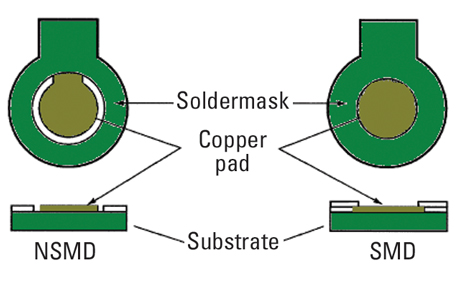
There are two types of land patterns used for surface-mount pads: non-solder mask defined pads (NSMD) and solder mask defined pads (SMD). Figure 1 shows the difference between the two.
NSMD pads have the solder mask opening larger than the pads, whereas SMD pads have the solder mask opening smaller than the copper pad. Most vendors suggest that NMSD be used because it provides tighter control of copper artwork registration compared to the positional tolerance of the solder masking process. Moreover, SMD pad definition may introduce stress concentration points that may result in solder joint cracking under extreme fatigue conditions. For NMSD, the pad size is typically reduced by 15% over the BGA diameter to achieve balanced stress on the solder joints. This method can also help to increase the routing channel on the primary layer.
|

FIGURE 1. The difference between an NSMD and an SMD Pad.
|
BGA Fan-out
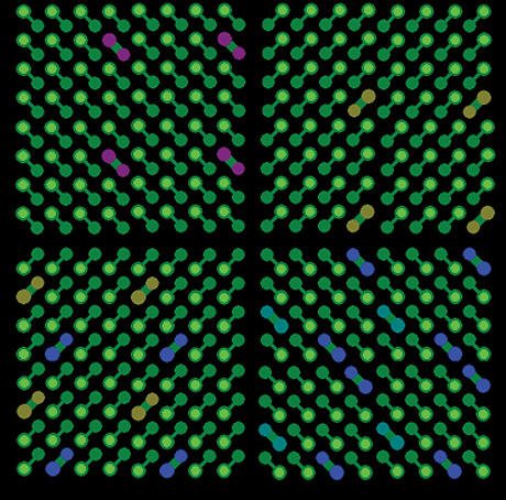
Modern device complexity requires the use of fine-pitch BGAs, which call for diagonal placement of via capture pads compared to in-line with the surface pads. Flared dog bone fan-out is the most popular method used today. It allows for better partitioning of the device into four quadrants. It also gives a widened channel for routing in the plus sign/cross region of the BGA, as shown in Figure 2.
|

FIGURE 2. Placement of via capture pad for 1.00 mm flip chip/BGA NSMD land pads.
|
Via pad size also affects the number of traces that can be routed within each channel. In Table 1 [PDF format], there are examples of conductor and space widths that fit between adjacent lands with various pitches and land diameter.
As seen from the table, the ability to perform escape routing is defined by the width of the trace and the minimum space required between traces. The channel area between adjacent via pads is the smallest area through which the signal must be routed.
Channel area CA = BGA pitch – d, where d is the via pad diameter.
The number of traces that can be routed through this area can be calculated using Table 2 [PDF format].
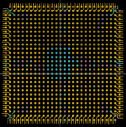
Once the designer has ascertained the trace and space width, the number of traces routed through one channel and the type of via used is established for the BGA layout, he can estimate the number of layers that will be required. The use of fewer I/O pins than the maximum can reduce the number of layers. If routing on the primary and secondary side is allowed, then the two outer perimeters can be routed without using vias. The next two perimeters can be routed on the bottom side as shown in Figure 3.
|

FIGURE 3. Using top layers for outer perimeters.
|
The remaining inner perimeters can be distributed among internal routing layers, and depending on the number of traces, routed within each channel internally. A fair estimate can be made by using the following simple formula:
Internal layers required = Number of Channels left ? Number of routes per channel.
A slightly lower trace width than that used on the top and bottom layers can be used on the inner layers to increase the number of traces that can be routed per channel. The trace can be necked down inside the BGA to a smaller width. This technique is acceptable for impedance-controlled traces in the megahertz range.
Specialized Techniques for Routing Fine-Pitch BGAs
For high performance and other system needs, designers can use premium technologies, with finer lines/spaces on board. When using fine-pitch BGAs, vias-on-pad technique may be implemented. The vias are placed directly on the BGA pads and filled with a conductive material, usually silver, which can provide a fairly flat surface.
As an aside, silver-filled vias represent a specialized process and extend PCB fabrication time by three to ive days and often result in additional cost. In the case of prototype build where silver-filled vias are involved, that additional week increases the usual four to six week prototype schedule by at least one week or so. In some instances, the only option is to use silver-filled vias. They are less expensive to fabricate compared to blind and buried vias. In some cases, compromises must be made between cost and manufacturing time.
In a BGA pad design using silver-filled vias, the need for dog-bone fan-out is eliminated, and a small increase in density is realized by being able to route a few more signals on the outer surface. In addition, discrete decoupling capacitors can be placed directly over the vias on the bottom side, providing a low inductance path to the power system.
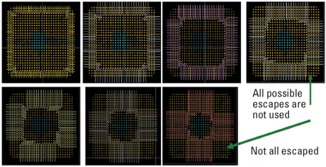
On 0.5 mm pitch BGAs, a microvia on the BGA land is the most common approach, as pads are not typically large enough for through vias. In this case, the outer perimeters can be fanned out using blind vias. Traces from inner perimeters can travel underneath these vias. This methodology can save an extra layer. When the number of layers becomes the driving factor in the design, the board designer has to improvise and make sure that most of the routing escapes are used and all the internal layers are fully utilized. Most of the time, the traditional approach is used, where every trace is routed orthogonically inside the BGA as shown in Figure 4.
|

FIGURE 4. Traditional approach where each perimeter uses a different routing layer.
|
Unless there are very strict signal integrity rules to follow, especially when the signal is in the GHz range, the only benefit that this technique gives is cleaner routing. There are no gains with regard to signal performance.
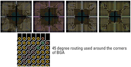
A more productive technique could be to route on a 45-degree angle from the corners of each quadrant. This method will aid in utilizing all possible escapes and, in turn, could reduce the number of layers required. Figure 5 shows the use of this technique in conjunction with a flared dog-bone fan-out method.
|

FIGURE 5. A better approach utilizing all trace exits in each routing layer.
|
Conclusion
As packages are able to handle more I/Os with a minimum increase in size, signal escape routing can be quite difficult to achieve. The number of PCB layers required to escape all the pins depends on a number of factors. Some of these factors, like the ball pitch and land size are device specific and need to be considered prior to starting the board layout process. The others have to be figured out by the designer. Board designers will always be pushed toward using the minimum number of routing layers to reduce cost, especially when using a strip-line structure. Therefore, successful and effective routing will always be a challenge for the PCB designer. PCD&M
Syed Wasif Ali, CID, is a layout engineer with Nexlogic Technologies Inc. For more information, contact This email address is being protected from spambots. You need JavaScript enabled to view it..
REFERENCES
1. High Pin Count BGA Routing Techniques. Hugh Allen, September 2005.
2. Designing With High-Density BGA Packages for Altera Devices, July 2006.
3. IPC-7095A, October 2004.


