When measuring the quality of a received signal, simulation tools provide a more accurate means to interpret what the receiver is seeing.
Source series termination is the most popular termination strategy for point-to-point connections and single-ended serial busses. If you try to measure the quality of the received signal, you often see a worse waveform that the receiver does. Being aware of the hidden complications of the measurement can help you back out the received signal quality.
In source series terminations, a resistor in series with the driver, combined with the series output impedance of the driver, terminates the signal line. This is shown schematically in Figure 1.
In this case, a signal entering the transmission line will hit the high impedance of the receiver and reflect back to the driver. This reflection from the receiver is not the problem. The problem is the reflection of this bounced signal off of the driver. There will be no reflection off the driver if the series resistor plus the output impedance of the driver matches the line impedance.
|

FIGURE 1. Typical source series termination schematic.
|
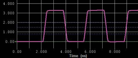
When done correctly, the receiver should see an acceptable received waveform with no reflections present, and the length of the transmission line will not affect the signal quality. Figure 2 shows an example of what is expected at the receiver.
|

FIGURE 2. Received signal with source series termination, 300 MHz clock. (All simulations done with Mentor Graphics HyperLynx).
|
But, when you try to measure this waveform, this is not always what you see. Three important complications hide the true signal the receiver sees from what you might measure.
The first complication is that you are rarely able to probe at the receiver. Instead, you typically probe at a BGA solder ball pad or at a test point located some distance from the package. This can be as far as 1" to 2" from the I/O pad of the receiver on the die.
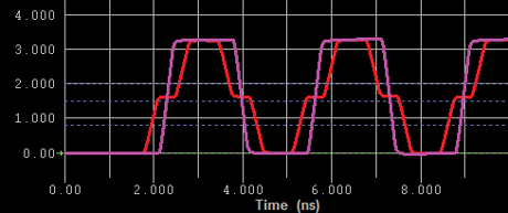
At this location away from the receiver, what you initially see is half the voltage of the unloaded driver, the injected signal, as it propagates down the transmission line. When it hits the high impedance of the receiver, this signal reflects, and you see the reflected voltage a short time later pulling the signal up to the full amplitude. This is shown in Figure 3.
|

FIGURE 3. Red trace: the voltage that would be measured about 2 inches from the receiver pad.
|
The second complication is that the input impedance of the receiver is rarely perfect high impedance. There is always some input capacitance associated with the I/O pad of the receiver, the ESD protection diodes and the package leads. This can be from a low of about 1 pF in well-managed devices to as large as 4 to 5 pF when care is not taken.
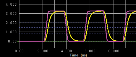
The impact from this capacitance on the receiver is to slow the edge down and add an effective delay of roughly 50 Ohms x 4 pF ~ 200 psec, which can be important in some applications. An example of the impact from 4 pF of input capacitance is shown in Figure 4.
|

FIGURE 4. Yellow trace: received signal with 4 pF of input capacitance.
|
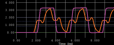
The presence of this 4 pF of capacitance will complicate the received signal at the test pad location. Its low initial impedance will cause a brief negative reflected voltage, as shown in Figure 5.
|

FIGURE 5. Orange trace: the measured signal located at a test pad, with 4 pF of input capacitance to the receiver.
|
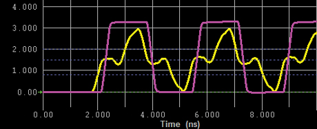
The third complication in a measurement arises from the type of probe used to measure the signal. Obviously, you can’t use a 50 Ohm probe to touch the test pad. This will completely load the line and be a disaster. But, even a high-impedance 10x probe, with typically a 500 Ohm input impedance and 2 pF of input capacitance, will affect the signal. Figure 6 is an example of what might be expected with such a probe.
|

FIGURE 6. Yellow trace: expected signal with 500 Ohm and 2 pF scope probe at test point with 4 pF of input capacitance.
|
If the signal shown in Figure 6 were the basis of judging signal quality, your design would probably fail. But, by using a simulation tool to map out what is actually measured, you can sometimes interpret what the receiver is actually seeing. Often, it is better than what can be measured. PCD&M
Send questions to This email address is being protected from spambots. You need JavaScript enabled to view it..
Dr. Eric Bogatin is president of Bogatin Enterprises.


