In-line automated loading and unloading allows low-volume, high-mix product testing to continue around the clock.
The changes in manufacturing processes and economics in many different companies, and the short times needed to go from design to the manufacturing of the end product, increasingly justify the use of automation to achieve the levels of efficiency and productivity dictated by today’s time and cost constraints.
Since test is part of the process, it is only natural that PCB test solutions need to address the issue of providing a high level of test coverage and diagnostics while providing real-time feedback to manufacturing and/or design in an automated way. Automation brings the added value of increased productivity, thus effectively lowering test costs. However, to be cost effective in many of today’s PCB manufacturing operations, characterized by a high number of different part numbers and low to medium production runs, any automated solution must have a very high degree of flexibility and a very low setup time. In order to achieve this, an automated solution must include the mechanical flexibility to allow the user to fully utilize it for high mix, low volume production as well as intuitive, streamlined software tools that optimize the time required for program preparation and system setup.
The goal, in regard to engineering a process to integrate an automated line, is to increase manufacturing efficiency, maintain high quality and to reduce costs in order to compete in the global market. This choice must also be compatible with today’s compressed new product introduction (NPI) cycles, which require a fully functional manufacturing process to be up and running in extremely short times. Generally speaking, the last step in electronic product manufacturing is dedicated to test. We will examine the possibilities to fully extend the automated choice also to the world of PCB test.
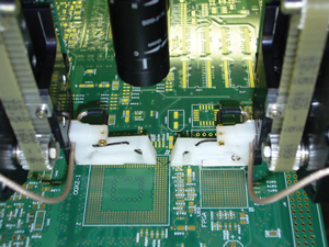
Of course automation has been available on traditional bed-of-nails test systems for quite a long time, but more and more companies are opting for flying probe test systems (shown in Figure 1) due to its many advantages. First of all there is no need to build and maintain a fixture for each product code, which means a considerable savings in money and time, not least by eliminating the need to “fight” against the typical fixture problems (bad contacts, dirty pins, storage space, etc.). Another advantage in terms of process optimization is that there is virtually no system setup time. To change to a different product code, the operator simply selects the required test program from the list of existing programs or, in the case of a new product, generates a new test program.
|

FIGURE 1. Flying probe tester.
|
Suitable Test Methods for Typical PCB Faults
PCBs coming from the manufacturing line can basically have two principal types of defects: short circuits between (and normally adjacent) tracks, which are commonly called “shorts,” and interrupted tracks, commonly called “opens.” The PCB test must therefore be aimed at detecting and diagnosing these two categories of faults.
The most exhaustive test method includes resistive measurements between one single track and all the others to detect shorts, and continuity measurements on all of the nets to detect opens. This is the approach commonly used on bed-of-nails systems, but the growing density and miniaturization of today’s PCBs are making it increasingly difficult to build fixtures that can access every test point. A flying probe system with sufficiently precise probing capability can solve the accessibility problem, but test time can become an issue on boards with a high number of nets.
An alternative test approach specifically designed for a flying probe test is present. Basically, capacitive measurements are performed between each single PCB track and a reference point, which can be a single track or a ground plane. These capacitive values are saved in a database to be used as “golden” values during testing of subsequent PCBs. These auto-learned values undergo an automatic certification procedure and only the certified values go into the database and are used to compare the values measured on the next PCB under test to determine whether or not the board is good or faulty.
Using this test method, the total number of measurements performed on the PCB decreases with respect to the traditional resistive/continuity method described previously, keeping test time down while maintaining the same level of fault coverage. From the test process point of view, this method presents numerous advantages: PCB batch testing can start immediately from the first PCB without the need for time-consuming setup procedures; test time is drastically reduced, allowing higher productivity; there is no need to have a “golden” board since the certification method builds its data base of good values during the tests of the different PCBs in the batch; and the PCB pad or test point is physically contacted only once by the probes, avoiding the mechanical stress of multiple probe hits required for a complete resistive/continuity test. These last types of tests are then used only where necessary to pinpoint the location of any shorts or opens found.
A Simple Software Process
Test program generation must be fast and easy in order to stay within the short time allotted for setting up the process. Starting from the information in the CAD/CAM files of the PCB, the test system must be able to import this data, converting it into a format that can be used directly for creating the test program. The standard format is IPC-D-356A, which includes all of the information about the PCB (nets denomination, track path, pad positions and shapes, information about any embedded components) needed to generate the PCB test program automatically.
The data import procedure should be simple and straightforward. On some systems, this procedure is integrated into a process-oriented environment that guides the operator through only three simple steps, allowing you to be ready to test the first PCB in a matter of minutes. A typical example that is found on the Seica S24 system follows:
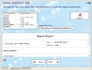
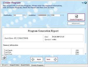
Step One – Prepare. A test wizard proposes the window for importing the CAM data, also enabling the user to define some test parameters that define the shorts and opens threshold values (Figures 2 and 3). The software then generates the test program automatically, providing a statistics report and showing all of the nets and pads that are taken into account during the test.
|

FIGURE 2. Import phase from CAD data.
|
|

FIGURE 3. Generation of test program during the preparation phase.
|
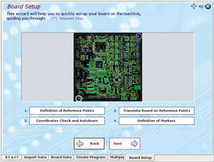
Step Two – Verify. At this point the user must physically place the PCB in the test system. Thanks to the data import procedure, the PCB information is graphically displayed (Figure 4). The operator must choose two reference points (also called fiducials) using the integrated camera to learn their positions. This process aligns the PCB and the test system. In fact, once this process is finished, the system can automatically calculate the correct physical coordinates of all points on the PCB.
|

FIGURE 4. The alignment between PCB and test system using the two reference points.
|
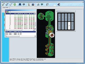
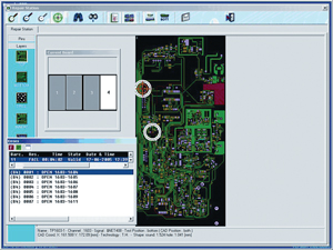
Step Three – Test. Now the user can run the test of the PCB. The test results in a pass or fail message, and any defects found, will be indicated in the test report. On some systems, the repair station environment helps the operator to locate the position of the failing net on the PCB, and includes statistics functions and procedures for the retest of the failures. A graphical display shows the operator the implicated tracks of the failing board with the relative internal layer and identifies the precise location of the defect with a flashing cursor (Figures 5 and 6).
|

FIGURE 5. The Repair Station graphical environment. The red and orange tracks are shorted together. The error is listed in the left dialog box.
|
|

FIGURE 6. The Repair Station graphical environment. The two white circles highlight an open circuit.
|
A Completely Automated Solution
Up till now, we have described possible solutions for minimizing the time and effort required to get a PCB test program up and ready on a test system.
In order to reach a fully automated test solution, it is necessary to choose a test system that can work in line with automatic loading/unloading capability. Since the time required for test is generally longer with respect to most of the other manufacturing processes, the most commonly used configuration for test is an island type, with external PCB magazine-loaders connected to the internal loader of the test system. Due to the growing requirement to handle low-volume, high-mix types of production, the optimum solution should be able to accommodate multiple product types and quantities to take full advantage of the 24/7 operating capability of an automated solution.
A simple software menu allows the user to set up the test sequence and then the test system will proceed to test each PCB, automatically adjusting the rails, loading the PCB and running the appropriate test program. After each PCB is tested, it is unloaded automatically and conveyed to separate storage shelves, according to the pass/fail test result, and the test data is automatically saved to a file for statistics and repair. Optional markers can also be provided to automatically stamp each PCB with the test result. The use of this type of automation solution reduces operator intervention to a minimum.
So, is it possible to fully extend the automated choice to PCB test? At this point, we would have to say yes; the technology is available, and the statistics show that a growing number of companies have made the choice to invest in this type of solution. Of course any kind of automation requires a higher initial investment, which is then offset by the higher productivity and lower operating costs in the medium/long term. On average, the 20 to 25% higher initial cost is recovered within the first year or sooner in a 24/7 manufacturing environment.
The automated solution we have described here can also be used to add a virtual second or third shift with regard to PCB test, since even those companies that operate on an eight-hour basis can take advantage of the off hours to test up to 100 boards, without the presence of an operator. PCD&M
Nicoletta Gianotti works in Seica’s technical marketing and communication department. She can be reached at This email address is being protected from spambots. You need JavaScript enabled to view it..


