Combining the intelligence and skill of an experienced designer with the speed of traditional autorouting tools.
Since the invention of the autorouter some 40 years ago, its use has been limited to large, digital multiple-layer printed circuit boards for the simple reason that an autorouter cannot mimic the intelligence of an experienced designer. Most designs are routed manually in industries where the resulting product must contain the densest routing and minimum number of layers to reduce final product cost. For example, in a high-volume product such as a laptop, the elimination of one layer can mean the difference between a competitive and non-competitive product price.
Other drivers for manual routing include maximizing system performance, manufacturability and sometimes just pure esthetics. This is especially true for the 8, 16, 32 and 64-bit buses that connect the major components of a design. The drawback of the manual routing process is that it is extremely time consuming and can significantly increase the design cycle time, thus putting undo pressure on the designer to meet a company’s aggressive time-to-market schedules. And most of the work in routing these buses is tedious once the plan for the buses has been established. Laboriously digitizing in the bend points of a 64-bit bus is not a good use of a designer’s time.
So why not use autorouters to perform this laborious part of the job and leave the designers to more efficiently apply their skill? The basic problem is that while an engineer or designer sees the problem at a higher level and can visualize the flow of buses and interconnects between components, an autorouter attacks the problem one interconnect at a time.
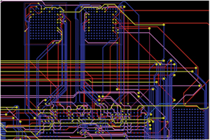
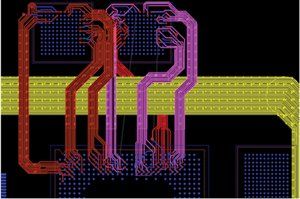
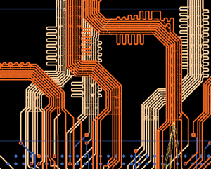
Figure 1 shows the result of an autorouter as it was applied to a set of small buses. The results of this autorouting may be electrically correct but lack in manufacturability, density and ease of change, to say nothing of esthetic form. Figure 2 shows that same set of buses as a designer would manually route them – denser, higher performing and much more esthetically pleasing. The planning and manual routing of these buses has followed a long established design process proven over the years to result in the densest, lowest cost and highest performance products. The process leverages the skills of both engineer and designer.
|

FIGURE 1. Routing done by an autorouter.
|
|

FIGURE 2. The same routing done manually by a designer.
|
The Classic Design Process
The established design process typically consists of two steps: planning and routing. When planning a dense PCB, engineers or designers typically sketch the physical bus systems and sub-system architecture on paper. This sketch tries to account for optimum component placements but rarely has any concept of bus widths, bus layer assignments (affects interconnect impedance), interconnect lengths (affects net delays), or layer congestion (may not fit on the desired number of layers). This paper plan is then used by the designer to perform initial major component placements while eyeballing the design to see if, in fact, there is enough space between the components to route the buses and if the desired net lengths (delays) are achievable. This planning process iterates the actual manual routing of the buses until a good solution is found. Although very labor intensive, the results are excellent. Then the dreaded engineering change order (ECO) materializes and design must iterate again.
So, how could the productivity of the process be significantly improved with automation while achieving results similar to the manual process? A long-time goal with autorouters has been to add automation to the designer skill to produce results that closely mimic a designer’s manual routing.
Automating the Planning Process
To combine the knowledge of an engineer, the skill of a board designer and the power of an autorouter, a powerful topology planning and routing technology has recently been developed. This technology provides automated planning tools for the engineer and designer to evaluate and plan bus-system interconnects early in the design process. The design plan is developed with a user-friendly tool to perform initial major component placements and to “sketch†in the bus paths. During this process, the buses take on their actual widths so it is easy to see if there is enough space for routing between the components.
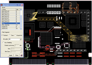
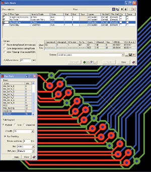
When planning the buses routing layers are assigned, enabling the calculation of impedance and net delays. If desired, the interconnects can be quickly routed using the autorouter so precise net delays and signal integrity issues can be resolved early in the planning stages to avoid costly design iterations. Once the topology plan is complete, it is stored with the layout design database. Figure 3 illustrates a sample design plan. The different colors represent different routing layers for the buses.
|

FIGURE 3. The bus topology plan is developed and captured by an engineer or designer.
|
Functionality in the topology planner automatically optimizes the interconnect sequences at the ends of the bus paths. For instance, if a 64-bit bus is split into two 32-bit paths, the planner will choose the best 32 interconnects for each path based on fan out lengths from the major components. This optimizes the final routing to achieve the shortest interconnect lengths and best net performance (delays).
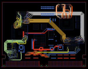
Once the plan is complete, the CAD designer can use the autorouter to route the connections following the plan. Instead of taking hours and even days to manually digitize in the buses, the autorouter can complete the task in minutes saving valuable design cycle time and significantly improving the productivity of the designer. Instead of spending time laboriously digitizing in bend points, the designer can apply time and talents to more productive tasks. Figure 4 illustrates the results of autorouting the design following the plan shown in Figure 3. These results are tightly packed, as a designer would do manually.
|

FIGURE 4. The results of autorouting the bus plan from Figure 3.
|
If the resulting routes do not meet designer approval or if the dreaded ECO occurs, the plan can easily be modified to reflect the change and the autorouter re-executed on that particular bus. So not only do designers save significant time on the initial design but iteration times are reduced as well.
The autorouter not only follows the bus path structure plan but also a set of rules (constraints) for high-speed delay and signal integrity, shielding, manufacturability and specialized designer practices. An example of this is the set of high-speed design rules. Here the bus nets are assigned rule classes that dictate their delays, crosstalk and signal integrity parameters. The autorouter follows these rules, but under an additional control by the designer. In this case the designer can specify where on the board the router can break from its dense patterns to accommodate the high-speed rules. The designer can specify a board area, and within this area the router adds length (trombones) to equalize the interconnect delays, or spreads traces to eliminate crosstalk (Figure 5).
|

FIGURE 5. The designer can specify board areas where high-speed tuning such as delay “tromboning†will occur.
|
Another typical control is for the shielding of nets. A rule can be specified for a bus to dictate the number of interconnects between each shielding net, for example four. The planning tool then automatically increases the size of the bus path and the autorouter puts a ground connection between the signal connections and connects the shield to the ground plane with a via (Figure 6).
|

FIGURE 6. Shielding of nets can be controlled in the plan and performed by the autorouter.
|
Also illustrated in Figure 6 is the changing of a layer by a bus following the plan. Here the plan has dictated the change of plane location and the via pattern to accomplish that change. Again, this mimics the way an experienced CAD designer would perform this task.
Design Re-use
A popular method of reducing time-to-market and to increase design quality is to re-use an existing design as the start of the next product. This is especially true in the consumer market where new products must be introduced every four to six months and the new product often consists of upgraded features from a previous design. A prime example of this is a cell phone where the new model may add a few features or upgraded memory to the previous model.
Since the topology plan and routing is stored with the rest of the design database, this information can be used to more efficiently start the next product design. Using this process, all or part of a design is stored and managed as a piece of the company’s intellectual property (IP). At the start of a new design, the IP is accessed by the new design team and used as a starting core. The core, including the topology plan and routing, is modified to reflect any new product requirements and then augmented with additional functionality. The results are significantly reduced design cycle time and improved product quality.
The topology planning and routing technology provides a unique way for the engineer, designer and autorouter to work together in planning and designing complex bus systems and avoiding the sketchpad instructions and hand-routed boards. It also complements the designer’s vision of logic flow while making ECOs easier to manage as bus paths can be quickly moved and re-routed while still maintaining design integrity. High quality/manufacturability routing is the result with reduced design cycle time. PCD&M
John Isaac is the director of market development, Systems Design Division at Mentor Graphics Corp. He can be reached at This email address is being protected from spambots. You need JavaScript enabled to view it..


