An investigation of blind and thru via fill techniques for semiconductor package and printed circuit board applications.
My conversations with Endicott Interconnect (EI) began in search of details about one of the technologies used in semiconductor packaging products (first level package) and printed circuit board (second level package) applications, via fill. EI offers both conductive and non-conductive versions of via fill, employing a number of diverse techniques that are dependent on the product type, specific design and customer requirement. What I learned in the course of this interview was more than just how and why EI fills some vias. The EI business model, coupled with their vertically integrated technology capability is filling the much bigger gap that exists for engineered interconnect system solutions in the medical, advanced test equipment, defense and aerospace markets. The company is leveraging a strong OEM heritage to provide a comprehensive electronic package to the high reliability market segments.
Everyone knows a bit about IBM history. One of the foremost OEMs in North America, IBM maintained captive printed circuit design, manufacturing and assembly capabilities into the 21st century, long after most of their competitors had outsourced these functions. In November of 2002, IBM decided to spin off printed circuit manufacturing. The newly formed and independently owned entity, Endicott Interconnect, began with minimal fanfare and much trepidation during one of the worst industry slowdowns on record. Four years later, it has diversified its product offering and opened its doors to an extremely receptive merchant market. From 2003 to 2006, the company’s sales have grown in excess of 55%. Their market diversification has shifted as well. In 2003 it was 85% IT/Telecom focused. In 2006 it is projected that only 50% of sales will come from IT/Telecom. The significant figure is that 25% of the 2006 sales will come from the defense and aerospace market that was only about 1% of sales three years ago.
In the area of process differentiation, EI builds on the technology development legacy created by IBM. EI manufactures its products using microvias and other enabling technologies. Microvias are incorporated into designs to solve density problems. EI uses different methodologies to generate filled vias in its products. EI can either plate copper metal to fill a via or use a laminating process to fill a via with epoxy. Alternately, EI will screen print filler into the holes with either conductive or non-conductive fill materials. These techniques generate filled vias that provide planarity for layer-to-layer connections. For PCBs (second level packages), filling vias or small through-holes is done primarily to solve manufacturing problems. In the case of first level packages, filling vias with conductive materials like copper can provide improvements in performance including lower inductance, lower electrical resistance and better thermal conductivity.
Via Fill for Semiconductor Package Applications
Electroplated copper via fill and other conductive via fill methods are used primarily on semiconductor packages. Here the use of microvias is critical to freeing up wiring channels as circuit densities increase. As the circuit density increases and pitch decreases, it becomes difficult, if not impossible, to route wiring without using stacked vias or vias in pads. As an example, at 150-µm pitch, there is not enough room to design with dogbones, therefore stacked vias are used to facilitate connection between the layers. With copper-filled stacked vias, one can achieve high package density and routability is extremely high1. Stacked vias free up real estate that can be used to increase wiring density without decreasing line widths to impractical levels that would significantly reduce yields.
When stacked vias or via-in-pad design are required there are a number of manufacturing options that can be used to fill the vias. In many cases the most straightforward approach is to fill the vias with copper, by electroplating. This works well in designs where the layers are thin and the vias are small. The resulting aspect ratios (typically 1:1) and uniform via sizes result in consistent via fill using plating methods. Alternatively, filling can be accomplished with a non-conductive material. This step is followed by overplating the fill material with a conductive layer. In either case, filling the vias makes the process of aligning and connecting the vias from layer to layer possible with reasonable manufacturing yields.
There are some electrical and thermal performance advantages to using copper filled stacked vias. There is a slightly lower inductance. In addition, conductive-stacked vias provide a more direct means for heat conduction. In some cases, three or more times the enhancement in thermal conductance is possible. Further, stacking vias reduces the electrical resistance as well as the thermal resistance. This offers the benefit of a reduced joule heating in high current density applications, thus improving the current carrying capacity of the via structure. Such benefits could be especially critical in high power and gaming applications, where every electrical and thermal advantage is often exploited in the design.
Manufacturing Considerations for Semiconductor Package Applications
Conductive fill, especially for packaging applications where vias are small (50 to 75 µm in size), is often completed using an electrolytic copper plating technique. The technology closely mirrors semiconductor channel fill where copper is plated in a bottom up fashion to fill sub-micron channels on silicon. To achieve plated via fill a specially formulated electrodeposited copper is applied to the board during an extended plating cycle. EI can fill a blind via that is 50 µm x 50 µm using electroplating techniques. EI achieves better than 85% hole fill depositing only 12 to 13 µm of copper on the surface. Throw power approaches 350%. The process is designed to fill the blind vias without plating thick copper on the surface. This eliminates the need for planarization, saving cost and reducing the number of process steps.
Via Fill for Printed Circuit Board Applications
Blind and buried vias in laminate structures need to be filled with something. Sometimes these vias can be simply filled with excess resin that flows during the lamination process. When joining thick panels however, where the volume of resin needed to fill the holes is high, additional measures may be required to avoid resin starvation between the sub-composite and the build up layer. In these cases an extra step is added that pre-fills the holes while they are in the sub-composite stage. This ensures that the holes are completely filled prior to composite lamination. The filled sub-composite vias are less likely to trap process chemicals, reducing the risk of contamination during the processing sequence.
Manufacturing Considerations for PCBs
At EI sub-composites are always filled with nonconductive materials to generate a planar surface before the next build up layer is added. The company uses an in-house developed, restricted flow lamination process to apply a patented formula of copper or silica-loaded epoxy to the sub-composite. The epoxy paste is cast onto copper foil to make a loaded resin-coated copper foil to EI specification. Available in 2.5 and 3.7 mil epoxy thicknesses, the resin is B-staged similar to standard RCF materials. The hole-fill resin has a long gel time and good flow characteristic to allow for filling high-aspect-ratio through-hole vias. EI uses an etched copper mask to selectively fill the holes. After lamination of the hole fill, the copper mask and copper foil carrier are removed and recycled. The sub-composite with resin filled holes is planarized through a chemical and mechanical polishing process. Other non-conductive fill of completed printed circuit boards is achieved by screen coating with thermal-cured epoxy-based materials that are applied and cured using standard methods.
Conductive paste is an alternative to plating fill when a conductive fill is desired. This would be more applicable to thick panels with high aspect ratios that plated fill would not easily achieve. A common approach uses a silver loaded paste. These metal loaded epoxy-based materials are applied with screen printing techniques to the through-holes. Holes are typically filled from one side, and then are tack dried. The opposite side is screened in a second application and final cure follows. Often a vacuum screen bed is used to assist in more uniform fill. In the case of screen printed via fill, surface planarization and sanding to remove unwanted surface contamination are required. EI uses a unique combination of chemical and mechanical polishing through a series of abrasive wheels. The result is a planar and uniform surface, eliminating the unwanted surface scratching that may negatively impact future imaging and line generation.
Implementation Hurdles
Nonconductive hole-fill, either at the sub-composite or final board stage, is a straightforward process using well-known and typically available materials and techniques. That said, even for basic hole filling, there is a cost. Additional steps and materials are required. The lowest cost processes utilize screen coating. Lamination processes, such as those used by EI add expense and additional steps, increasing cycle time. Data generated by EI supports the value of the additional expense, especially for high reliability boards.
Plated conductive via fill is a more involved process. In a majority of cases process changes are required in both the electroplating chemistry and equipment to be successful. For EI the cost of the chemistry for hole-fill is higher than for their standard electroplating process. It is also a longer process because plating rates are slower. When the design calls for stacked vias, these are manufactured using a sequential process that adds even more process time. In addition, because the sequential manufacturing process involves building layers repetitively around a central core, yields can be negatively impacted.
Plating conductive via fill often requires a new equipment set. This may involve the entire plating system. Some processes work best with insoluble anodes because they are cleaner, create less nodules and reduce the required maintenance that would be needed if soluble anodes were used. Using insoluble anodes, however, add to the overall operating cost. Tank configuration may need to change and airflow, solution flow and rack agitation all play a more significant role in plated via fill applications. The initial seed layer contributes to the overall success of the process. Thin electroless copper alone, or direct metallization should be followed with an electrolytic strike plate to improve later via fill.
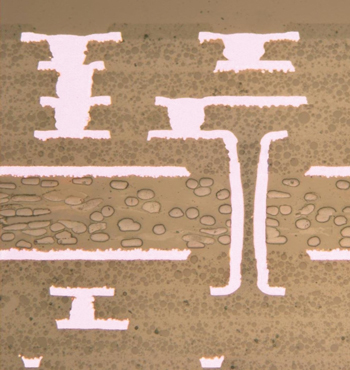
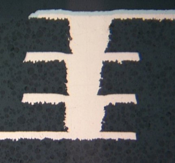
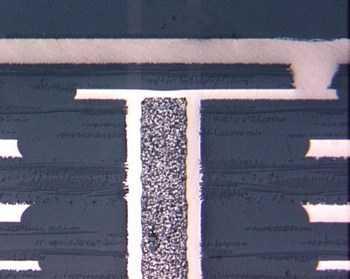
Process control involves solution monitoring, using cyclical voltammetric stripping (CVS), and wet analytical techniques. Specialized analysis tools have been developed to control plating baths used in the semiconductor channel fill applications previously mentioned that could be adapted for use. Currently the quality assurance of the plated filled product is accomplished by visual inspection. EI understands the arduous nature of this task, especially with tens of thousands of tiny filled microvias per panel. They are working on an automated AOI technique that isn’t prone to identifying false failures. Final testing and qualification includes cross sections (Figure 1, 2 and 3) that provide detail of the hole-fill quality and current induced thermal cycle testing (CITC), an in-house test developed to measure plated through-hole and via reliability2.
|

FIGURE 1. Cross section of printed circuit manufactured by sequential lamination technique using both laminated EI formulated epoxy hole-fill and copper plated via fill.
|
|

FIGURE 2. Cross section of stacked vias manufactured using copper plated via fill.
|
|

FIGURE 3. Cross section of a thick PCB that uses low-CTE sub-composite via fill plus a copper plated via fill for the microvia on the surface of a polyimide PCB.
|
In general the cost of filling vias is higher than the cost without hole-fill. Many designers and OEM customers believe that the small improvements that via fill provide come free of charge. This is a misconception. Depending on the type of fill and the number of additional processes that need to be undertaken to fill vias, the cost impact can range from an additional one to 10% more, plus there is a potentially negative impact on yields. There may also be capital requirements. So, choosing to design with conductive filled vias or requiring nonconductive fill for boards will affect the cost of the circuit and may limit the number of potential fabricators.
Summary of Advantages
The primary reason vias are filled is to improve overall product planarity or to make the space occupied by the vias usable at the next plane, either as a conducting pathway, or a layer on which to build more circuitry. There is a perception that filled vias, especially those filled with a conductive material, improve via reliability. The data collected by EI does not necessarily support this theory. Conductive or low-CTE nonconductive materials can sometimes simply move the location of failure from one point to another, yielding the same or even slightly lower via life than the original unfilled via. However, since there are no unfilled vias in a complex sub-composite board, EI has found that pre-filling does improve overall reliability since a good fill material always gives better via life than resin fill alone. Pre-filling also avoids other laminate problems related to resin starvation, as discussed earlier. There is also incidental evidence that filled vias improve the assembly process and can minimize voiding during solder attachment to via-in-pad structures. Therefore, at the end of the day, the correct hole-fill for each particular PCB is primarily there to enable the complex construction while maintaining high reliability.
Some physical benefits that can be gained by hole-fill are improved vacuum handling through assembly, because the panel has no “holes,” or easier-to-clean assemblies without small holes that can trap contaminants. A majority of the applications described for printed circuit boards are driven by the fabricator. These would include filling sub-composites to improve planarity and avoid resin starvation, and filling surface microvias with copper if the panel will be chemically or mechanically planarized later to reduce the copper foil thickness for improved fine line generation.
For packaging substrates, the advantages are much easier to quantify. In these applications, conductive filled vias are most common. There are definite benefits afforded by the use of conductive filled vias in these products. To efficiently design and route wiring, stacked copper filled vias have become a necessity. The space constraints caused by the packaging substrates are driving the adaptation of designs such as stacked vias that use conductive filled vias. Most of these conductive filled vias are manufactured using copper electroplating techniques. Copper-filled vias have inductance, electrical resistance and thermal advantages. Implementation can lower noise and reduce voltage requirement. Designers can look at a copper-filled blind or through-hole via as another tool in their design tool kits to achieve their performance goals. Modeling will allow them to consider the impact of the solid copper feature as it relates to inductance and capacitance, thermal dissipation and signal integrity in their designs. PCD&M
Ed. – For more information about Endicott Interconnect, see a companion article in the January issue of Circuits Assembly, “America’s Best Manufacturer?” by Mike Buetow, available on http://circuitsassembly.com/cms/content/view/4337/95/.
Kathy Nargi-Toth is editor of Printed Circuit Design & Manufacture; This email address is being protected from spambots. You need JavaScript enabled to view it..
Acknowledgements
Many thanks to Endicott Interconnect for the time and effort undertaken to provide me insight into the manufacturing process and design considerations for via fill. Special thanks to the members of the first and second level packaging product, reliability engineering and manufacturing teams for their assistance and patience in the writing process.
References
1. Varaprasad Calmidi, “Thermal Performance of a Thin High Interconnect Density Organic Substrate for Flip-Chip Applications,” Electronic Components Technology Conference, May 2005.
2. Kevin Knadle and Virendra Jadhav, “Proof is in the PTH – Assuring Vias Reliability From Chip Carriers to Thick Printed Wiring Boards,” Electronic Components Technology Conference, May 2005.


