 Many flex designs perform well with panel plating for countless bend-to-install applications.
When copper-plating vias and through-holes, there are several process options in the PCB manufacturer’s toolbox. Typically, they fall into three buckets: panel plating, pattern plating and button plating.
Panel plating (FIGURE 1) means the entire panel surface and all the holes will be electrolytic copper plated to the full plating thickness requirement. The etch process will etch down through the base and plated copper, leaving a pattern with features comprised of both the base and plated copper. Pattern plating is accomplished by creating a pattern of all the circuitry on the two exposed layers with a plating resist, then plating up the pattern of the outer layers. After stripping the resist, the etch process will etch away the base copper between all the plated patterns, leaving a pattern with features comprised of both the base and plated copper. Panel and pattern plating essentially result in the same end-product. For this discussion, we will compare button plating and panel plating.
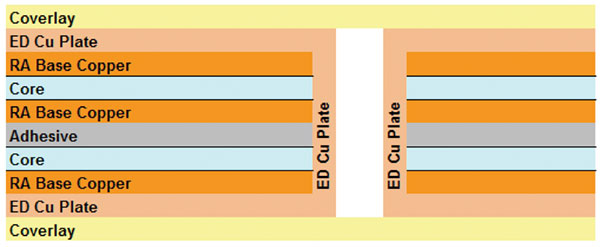
Figure 1. Panel plate.
Button plating is accomplished by creating a pattern of plating resist openings only at the holes, then plating up only pads at the holes. After stripping the resist, the etch process will etch away the base copper to create the etched pattern of just the base copper with raised pads or buttons at the holes (FIGURE 2).
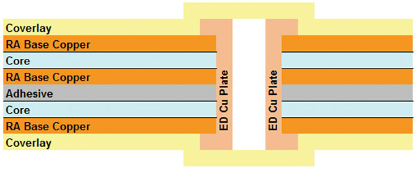
Figure 2. Button plate.
As a designer, there are situations to button plate rather than panel or pattern plate. Button plating will result in a thinner part in the flex region, with less copper, resulting in more flexibility. Thinner copper may also permit a thinner coverlay adhesive, helping to reduce overall flex thickness even more. This is important when the assembly has a tight bend radius or is expected to be bent many times over the product life.
Another consideration is the performance difference between rolled annealed (RA) copper and electrodeposited (ED) copper. Historically, RA copper has been softer and more pliable than ED copper. As a result, RA copper can be counted on to provide higher ductility and therefore more flexing endurance than ED copper. However, in recent years the performance of ED copper has improved dramatically, so the ductility of ED copper is much closer to that of rolled annealed. Another factor to consider is that by the time the circuit is fabricated, ED copper has been annealed to some degree after being exposed to various lamination and baking operations. In all cases, however, the grain structure of RA copper lies flat, while the ED copper grain structure stands vertically.
Some say all flex circuits should be button-plated, but experience reveals many flex designs are very successful with panel plating for countless bend-to-install applications. Button plating can marginally increase the unit pricing due to extra processing steps. In some very cost-sensitive applications, panel plating may help manage price.
Manufacturers may want to select button plating in some situations as well. As the etch pattern gets smaller and smaller, plating thickness variations may impact the ability to etch that pattern with acceptable yields. By button plating, the manufacturer can control copper thickness and thus improve etch yields. Another driver may be controlled impedance. Thinner copper traces result in higher impedance, so button plating can help meet higher impedance requirements. In addition, button-plated layers will etch more consistently, reducing variation in impedance values, which can be important.
Finally, many HDI designs drive button plating. The very fine features are hard to define with thick copper. When microvias are plated full, it is usually done with a button plate process to minimize the amount of copper on the surface. Also, certain layers may be plated multiple times due to the use of several via structures. This can result in excessively thick total copper, making etching difficult. In these cases, button plating may be coupled with flash plating to build up plating in holes without fully plating the surface.
As a designer, a key detail to keep in mind is the finished copper thickness. A panel-plated layer has thicker copper than a button-plated layer. This will impact current carrying capability and voltage drop over the length of the conductors. Also, lacking any specific instructions, the manufacturer may decide to either button plate or panel plate in order to achieve the best overall yield.
With the varying drivers for plating processes, a successful design strategy is to define the nominal finished copper thickness for the layers. This can help avoid unmet expectations if a particular copper thickness is needed for certain layers.
To summarize, either button or panel plating may be used successfully. The key is to understand how the plating option will impact the finished product.
Nick Koop is senior field applications engineer at TTM Technologies (ttm.com), vice chairman of the IPC Flexible Circuits Committee and co-chair of the IPC-6013 Qualification and Performance Specification for Flexible Printed Boards Subcommittee; This email address is being protected from spambots. You need JavaScript enabled to view it.. He and co-“Flexpert” Mark Finstad (This email address is being protected from spambots. You need JavaScript enabled to view it.) welcome your suggestions.


