New low-loss, optically stable materials can be manufactured using conventional PCB methods.
From cloud hosting to streaming mobile apps, the flow of data is exploding worldwide. According to Cisco’s most recent Global Visual Networking Index, global IP traffic will grow at a compound annual growth rate of 23% from 2012 to 2017. Indeed, annual global IP traffic will surpass the zettabyte threshold (1.4 zettabytes) by the end of 2017, reports Cisco. That is the gigabyte equivalent of all movies ever made crossing global IP networks every 3 minutes.
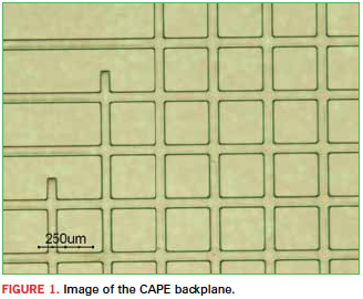
Yet mobile represents only one part of the total overall groundswell of data that, collectively and at the board level, is pushing conventional copper interconnect technology to its limits. The trend has sparked aggressive and much-needed development of board-level optical interconnect using either short fiber links or polymer waveguides. Both approaches can enable significant leaps in bandwidth while also reducing energy consumption and cost per bit transmitted. However, the cost and complexity of system assembly for polymer waveguides can potentially be much lower than short fiber links because waveguides can be integrated into the PCB rather than assembled on top. Polymer waveguides also offer significantly higher bandwidth density, as they may be placed much closer together than fibers, especially in fiber connectors. And waveguides permit more complex layouts by enabling fabrication of coplanar crossings in a single-layer of polymer waveguide, which is not possible with copper or fiber
(Figure 1).
All this is good news for the PCB industry, as the value of boards will greatly increase with the integration of optical functionality. But the path forward will require collaborative development along the entire optical interconnect value chain – from materials innovators to PCB manufacturers to computing platform developers.
The collaboration needed to advance this technology was underscored recently through the development of flexible polymer waveguides by IBM and Dow Corning.
Based on high-performance optical-grade silicones, the waveguides demonstrated excellent thermal and optical stability during and after board manufacture, and were successfully fabricated on flexible polyimide substrates. Moreover, these waveguides can be fabricated using conventional film processing and photolithography techniques suitable for manufacturing scale-up.
Polymer optical waveguides are not a new field of research. Early prototypes date to the 1970s, when industry and academia experimented with optical fibers constructed from liquid-core hollow glass. During the ’80s the focus turned to plastic optical fibers based on polymethyl methacrylate (PMMA) and later polyimides (PI) and polystyrene (PS) as the core material. Today, plastic-core fiber is used in numerous cost-sensitive communications applications.
But it wasn’t until the past decade that optical interconnect emerged as another promising market opportunity for polymer waveguide technology. With new opportunities, however, optical interconnect applications also presented unique challenges. High-performance computers and data centers impose thermally stressful environments that do not present a challenge for conventional copper interconnect. But sustained over time, such heat can typically degrade the physical and optical performance of transparent organic materials.
Indeed, candidate polymers for optical interconnect must endure even higher temperatures before they leave the manufacturing line, as Pb-free solder reflow processes often expose PCBs to temperatures reaching 260°C. In addition to these critical physical properties, polymers targeting optical interconnect applications must support use of existing tools and techniques for PCB manufacturing.
These demands all point to polymer waveguides based on optical-grade silicones as a promising, and even optimal, solution for optical interconnect. As a class of advanced materials, optical silicones deliver low loss at the wavelengths typically used for data communications’ excellent thermal stability, easy processability and photopatternability and superior chemical resistance. In addition, the modulus of these materials can be engineered to permit fabrication of waveguides on flexible substrates, permitting a much wider range of assembly and alignment techniques to be employed.
Fabrication Process
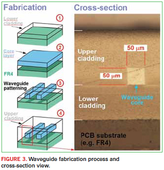
The recent collaborative successes by Dow Corning and IBM underscore the potential of silicone technology for optical interconnect applications. The waveguides are fabricated by first depositing a layer of bottom clad material. On top of this, a layer of core material with lower refractive index is deposited and UV patterned through a mask or with a direct write laser to create the desired layout. Finally, a top clad layer is added so that the cores are surrounded by higher index clad material. This enables light to propagate along the core through total internal reflection as with optical fibers (Figure 3).
The recent advance by Dow Corning and IBM builds on earlier collaborations, wherein polymer waveguides were fabricated on rigid substrates, such as silicon or FR-4 PCBs. These waveguides demonstrated propagation losses lower than 0.05 dB/cm at 850 nm.1 There was also minimal impact on the core material’s optical losses, even after exposure to accelerated aging at (85˚C and 85% relative humidity) for over 3,000 hr. and simulated solder reflow cycles.1
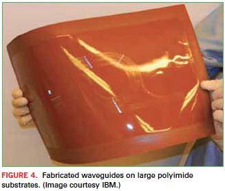
The relatively brittle nature of the silicone clad used in early experiments did not permit fabrication of waveguides on flexible substrates, however. A flexible waveguide layer can ease alignment and connectivity of optical components, and has the potential to produce highly integrated electro-optical configurations on flexible PCBs that can be assembled into space-limited 3-D design implementations (Figure 4).
A new clad formulation features core material used in the recent work that was effectively the same material used in previous research and development. Both materials are fast curing, enabling fabrication of waveguides in less than 45 min., 30 min. of which is a final bake step.
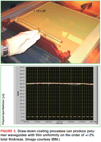
Exact process steps can vary. The material may be cast using spin coating or using draw-down coating methods such as doctor blading. Spin coating quickly produces waveguides with good dimensional control, but does not scale easily to produce large-area panels. For this, draw-down coating is more effective, and can provide film uniformity on the order of +/-2% total thickness (Figure 5). The doctor blade process is slower than spin coating when attempting to achieve layers of similar thickness, but more efficient when coating larger substrates. Both methods result in very similar waveguide structures, indicating this technology holds great promise for increasing process flexibility and overall manufacturing ease.
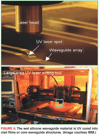
Curing of the wet silicone material to form clad films or core waveguide structures begins with application of ultraviolet (UV) light, followed by thermal setting of the material in an open air environment. The maximum absorption peak of photo-initiation occurs at a wavelength of 383nm. But, the material easily cures using either a broad-band UV light source, or a single wavelength laser emitting in the near-UV. A 2-min. bake on either a ceramic hot plate or convection oven at temperatures ranging from 110° to 130°C is enough to soft-cure the material. This permits it to retain integrity during processing of subsequent layers. A final 30-min. bake at 130°C stabilizes the cured material to ensure long-term reliable performance.
Patterning of core waveguide features has been demonstrated with noncontact mask lithography using a high-pressure mercury lamp and direct laser writing with a tripled Nd:YAG laser. Mask lithography produces well-defined features, but the size of the mask may limit its application to smaller substrates. Direct laser writing can produce waveguide features with comparable resolution to lithography. However, vibration, power density, writing speed and the number of passes are all manufacturing considerations.
Validating Mechanical, Optical and Environmental Performance
The flexible polymer waveguide technology showed mechanical, environmental and optical performance that meets IBM’s requirements. Waveguides constructed on flexible PCB-compatible substrates, such as polyimide, and bent into loops of 3cm diameter showed no relevant bending loss.1 Indeed, total propagation losses for these waveguides were very low and uniform, and ranged from 0.046 to 0.050 dB/cm.1
The material’s adhesion to polyimide substrates demonstrated that it is strong enough to withstand mechanical cutting processes without cracking or delamination. Pre-treatment of the substrate can improve adhesion if necessary.
Waveguides fabricated on flexible substrates at a thickness of 130µm demonstrated they could be bent around a mandrel with radius under 5mm without cracking or delamination from the substrate. They showed the same durability when twisted. Further, the waveguides showed no cracking when subjected to 500 cycles of dynamic bending around a 5mm radius.
The polymer waveguide material withstands common environmental factors in PCB manufacture, including solder reflow, with no measurable change in either insertion losses or attenuation.1
Conclusion
Material and manufacturing challenges confronting board-level optical interconnect are not insignificant. However, new polymer waveguide silicones are showing promise in resolving them, are compatible with rigid FR-4 and flexible PCBs, and can be manufactured using standard PCB manufacturing methods.
Work remains. IBM and Dow Corning demonstrated that a reliable optical waveguide technology can be built on flexible PCBs, and will continue to explore the aggregate bit rate, energy consumption and data density these new system designs can deliver. In parallel, Dow Corning is continuing to improve the performance, processability and volume scalability of the materials.
References
1. Brandon W. Swatowski, Chad M. Amb, Sarah K. Breed, David J. Deshazer, W. Ken Weidner, Roger F. Dangel, Norbert Meier and Bert J. Offrein, “Flexible, Stable, and Easily Processable Optical Silicones for Low Loss Polymer Waveguides,” Photonics West, February 2013.
Simon B. Jones is business builder, Dow Corning Polymer Waveguide Silicones; This email address is being protected from spambots. You need JavaScript enabled to view it.. Dr. Bert Jan Offrein is manager Photonics, IBM Research GmbH.


