Nine considerations to prevent signal degradation due to crosstalk and EMI.
With demand growing for AI chips the need for high-speed PCBs is on the rise. As operating frequencies increase over 10GHz, the risk of reflections, crosstalk and EMI increases.
For optimal performance, all frequency components of a signal should maintain consistent amplitude changes. Additionally, signals must reach their destination simultaneously to prevent phase discrepancies. Understanding these aspects will help the design of circuits without signal distortion.
Here we review the nine factors that lead to signal integrity issues and ways to mitigate them.
Downsides of poor signal integrity in high-speed PCBs. Inefficient signal transmission in high-speed circuit boards might affect the system’s overall functionality and reliability. Figure 1 depicts how noise hampers signal quality.
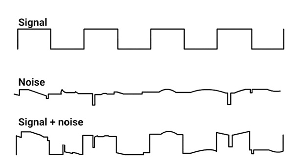
Figure 1. A signal with noise waveform at the receiver.
Here are three adverse effects of poor signal integrity in high-speed PCBs:
- Low signal-to-noise ratio (SNR). The SNR measures signal strength relative to noise level. When signal integrity is compromised, the ratio decreases significantly.
- Mismatched propagation delay (tpd). Propagation delay variation is a major concern when dealing with a group of signals. Poor signal integrity in high-speed PCBs can lead to inconsistencies in the time taken by signals to travel from source to destination.
Elevated electromagnetic emission and susceptibility. If a signal becomes susceptible to electrical noise, its quality worsens. Additionally, a distorted signal can induce EMI in the neighboring or connected electrical circuits.
Causes of Signal Degradation in PCBs
1. Impedance discontinuity. When transmission line impedance changes abruptly along its path, a part of the signal reflects toward the source rather than continuing to the destination.
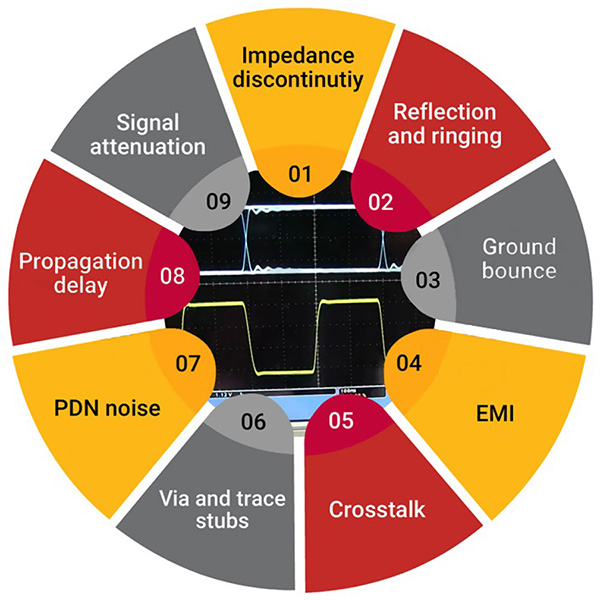
Figure 2. The nine factors that can cause signal degradation.
Impedance mismatches generally occur in these locations.
- Starting and terminating ends of a signal
- Intersection points of a signal with a via or connector pin
- Signal branches
- Via and trace stubs
- Splits in the return path or reference plane, as shown in Figure 3.
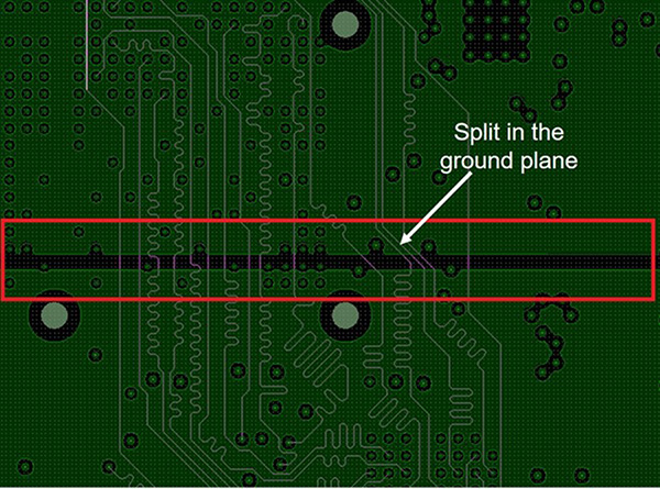
Figure 3. A layout image showing splits in the ground plane. This causes impedance discontinuity.
How to achieve uniform impedance in a PCB layout:
- Ensure consistent trace width, thickness and spacing along the signal transmission path.
- Route traces in a daisy chain fashion. A daisy chain trace routing refers to connecting components in series, one after the other, rather than multi-drop branches.
- Incorporate a series termination resistor at the source end and a shunt termination resistor at the load end for signal integrity.
- When routing signals over two reference planes, incorporate stitching capacitors to achieve a continuous signal return path (Figure 4).
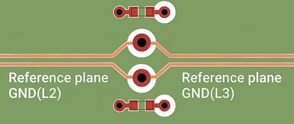
Figure 4. Adding stitching capacitors over two reference planes can achieve uniform impedance.
2. Reflections and ringing. When impedance is not consistent in a circuit, signals can reflect toward the source and interfere with the transmitting pulses. This interference can cause oscillating voltage or current, leading to ringing, overshooting (the signal exceeds its steady state), and undershooting (the signal is lower than its final value).
Consider these strategies to reduce reflections in a design:
- Place a damping resistor near the source to reduce reflected signal amplitude and prevent it from interfering with the original signal.
- When a signal changes its reference plane, place transition vias close to signal vias to maintain a continuous return path (Figure 5). Transition vias provide direct routes for signals to switch between different reference planes.
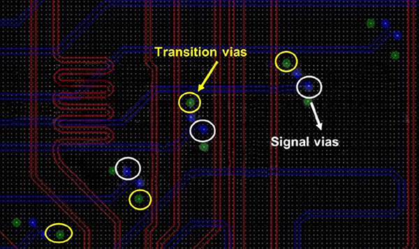
Figure 5. Transition vias near the signal vias.
- Keep trace lengths as short as possible, especially in high-frequency circuits where even small inductances can cause substantial issues. Long traces can act as antennas, increasing inductance and causing reflections.
- Use series or parallel termination resistors to match the transmission line impedance with the impedance of the connected components.
- Series termination: Place a resistor in series between the driver and transmission line. Position the resistor close to the source to match the driver’s impedance with the trace characteristic impedance.
- Parallel termination: Place a termination resistor in parallel with the receiver to reduce signal reflections at the load end (Figure 6).
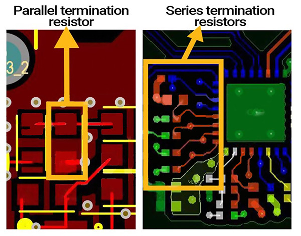
Figure 6. Parallel termination and series termination resistors to prevent reflections and ringing.
3. Ground bounce. Ground bounce occurs during transistor switching, causing the circuit’s reference level to shift from its original state (Figure 7). This shift is primarily due to impedance mismatches between ground rails and signals.
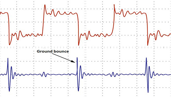
Figure 7. Ground bounce in an oscilloscope waveform.
Techniques to decrease ground bounce:
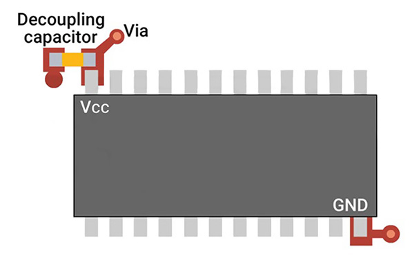
- Place decoupling capacitors near the power pin to stabilize voltage levels (Figure 8). These capacitors act as local charge reservoirs, providing instantaneous current to the circuit during switching. They reduce voltage fluctuations and the impact of ground bounce.
- Incorporate current-limiting resistors in series with switching transistors. These resistors limit the current flow during switching events, reducing voltage drop across the ground rails.
- Provide dedicated vias and traces for ground connections to ensure a low-impedance return path. Shared vias and traces can introduce additional impedance, leading to significant ground bounce during switching.
4. Electromagnetic interference (EMI). EMI occurs when energy is transmitted through radiation or conduction from one electronic device to another. It is caused by
- Electromagnetic emissions, or energy radiated from an electronic device, and
- Susceptibility to EM radiation, or the tendency of an electronic device to be affected by external electromagnetic energy.
To lower EMI in a circuit board layout
- Employ a Faraday cage, or a continuous copper fill around sensitive circuitry. It acts as a shield and blocks electromagnetic fields from escaping or entering the confined circuit.
- Implement via stitching along the edges of a ground plane or around critical signal traces to provide multiple low-impedance paths to the ground.
- Avoid discontinuities in the ground plane. Any splits or gaps can create unintended antennas that emit or receive EM radiation.
- Shield cables with conductive material that acts as a barrier to electromagnetic fields. This reduces the likelihood of interference.
5. Crosstalk. Crosstalk occurs when two adjacent conductors are close together, permitting energy to couple from the aggressor to the victim trace (Figure 9).
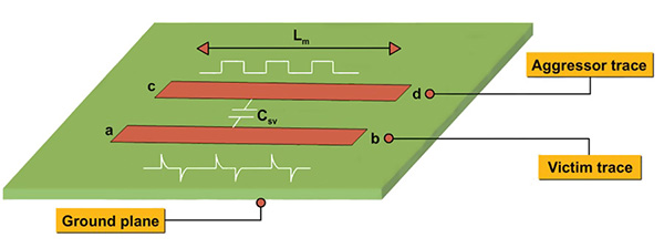
Figure 9. Mutual coupling between aggressor and victim traces.
When current flows through a conductor, it generates a magnetic field around it. If another trace runs parallel to the first one, the changing magnetic field induces a voltage in the adjacent trace. This effect is more pronounced when the traces are close together. High-speed digital signals, clock lines and analog signals are particularly susceptible to crosstalk.
The best practices to reduce crosstalk include
- Ensure sufficient spacing between adjacent signal traces. The recommended clearance is typically three to five times the trace width to minimize electric field coupling (Figure 10).
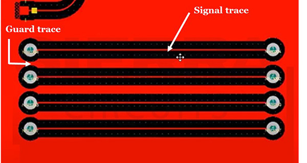
Figure 10. Spacing of 3W to 5W between guard and signal traces can avoid crosstalk.
- Place signal planes close to ground planes (preferably one dielectric away). Ground planes act as shields, providing a low-impedance return path.
- Route traces perpendicular to each other between layers to further reduce the chance of crosstalk.
- Avoid overlapping critical signals (such as clock lines or data buses) on adjacent planes.
- Add guard traces next to critical signal lines. They are beneficial when dealing with sensitive, high-frequency signals.
6. Via and trace stubs. Via stubs are the unused portions of vias that can act as resonant circuits, leading to reflections and signal attenuation.
To avoid via stub impact
- Ensure the maximum frequency is far less than the fundamental resonant frequency of the stub.
- Back-drill the vias with a slightly larger drill bit to remove the unused via portion.
Trace stubs act like antennas, radiating energy and causing reflections. To avoid trace stubs
- Adopt daisy chain routing. This involves routing the traces in a continuous chain, connecting each component in series rather than creating branches or stubs.
- Use series termination resistors at the driver end of transmission lines.
- Keep trace lengths as short as possible. Shorter traces reduce the potential for stubs and the associated signal integrity issues in high-speed circuit boards.
7. Power distribution network (PDN) noise. PDN noise arises due to the switching activity of devices’ output signals and internal gates. To avoid this
- Place power and ground planes in proximity. It reduces parasitic capacitance and inductance between planes.
- Choose IC packages with shorter lead lengths. Shorter leads reduce inductance and resistance in the PDN.
- Use multiple low-inductance decoupling capacitors of the same value (Figure 11). Place them as close as possible to the ICs’ power pins. These capacitors filter noise and provide a stable power supply to the ICs.
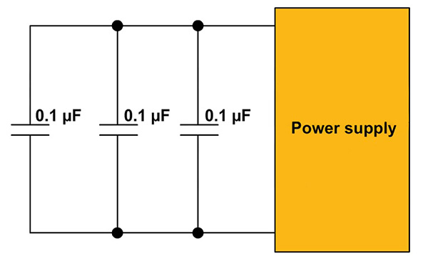
Figure 11. Placing multiple decoupling capacitors in parallel with a power supply to prevent PDN noise.
8. Propagation delay. Propagation delay occurs when data signals and clock signals do not arrive at the receiver simultaneously, causing signal skews. Excessive skew can lead to signal sampling errors.
Strategies to reduce propagation delay include
- Adjust trace width and spacing to ensure uniform impedance.
- Match signal lengths using serpentine traces (Figure 12). This ensures signals traveling through different paths reach their destination at the same time, minimizing skew and reducing the risk of signal sampling errors.
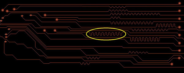
Figure 12. Adding serpentine traces to match line lengths.
9. Signal attenuation. Signal attenuation refers to the reduction in signal amplitude caused by conductor and dielectric losses. Conductor loss increases with trace resistance and frequency, while dielectric loss is influenced by the dissipation factor and loss tangent (Figure 13).
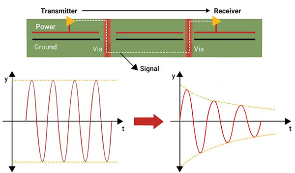
Figure 13. Signal attenuates with time while traveling from transmitter to receiver.
Design tips to mitigate signal attenuation include
- For signal integrity in high-speed PCBs, use a PCB material with a low-loss tangent and a low dissipation factor. Materials such as FR-4 might be suitable for lower frequencies, but for high-frequency applications consider advanced materials.
- Using very-low roughness profile copper foils, such as very-low-profile (VLP), hyper- very-low-profile (HVLP) and reverse-treated foil (RTF). These foils have smoother surfaces, reducing skin effect losses at high frequencies.
Signal integrity analysis using simulation and an oscilloscope (Figure 14). Simulation helps demonstrate the circuit board’s actual behavior before fabrication. It identifies root causes of signal degradation early in the design process, saving time. S-parameters, eye diagrams and a time-domain reflectometer can be used to perform signal integrity analysis.
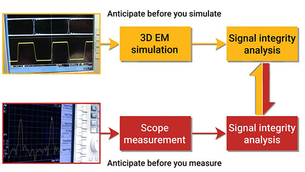
Figure 14. Signal integrity analysis using simulation software and oscilloscope.
S-parameters show how a signal propagates through an electrical network and represent its bidirectional behavior at input and output ports. They are saved in Touchstone files, standard formats for storing network parameter data. Their significance and application in signal integrity analysis are as follows:
- S11: reflection coefficient: S11 represents the reflection coefficient at port 1. It indicates how much of the input signal is reflected to the source (return loss). A high return loss (low S11 value) means that most of the signal is transmitted through the network with minimal reflection.
- S21: transmission coefficient: S21 represents the transmission coefficient from port 1 to port 2. It shows how effectively the signal is transmitted through the network. A high S21 value (low insertion loss) indicates efficient signal transmission with minimal loss.
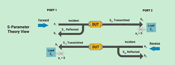
Figure 15. 2-port S-parameter analysis for signal integrity measurement.
Mixed-mode S-parameters provide insights into differential and common-mode behavior of differential signals. Figure 16 shows a four-port measurement with 16 S-parameters.
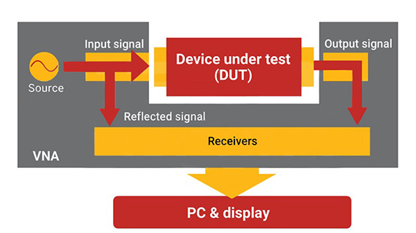
Figure 16. S-parameter measurement using a VNA.
- S31 = Near-end crosstalk from port 1 to port 3
- S32 = Far-end crosstalk from port 2 to port 3
- S41 = Near-end crosstalk from port 1 to port 4
- S42 = Far-end crosstalk from port 2 to port 4
A vector network analyzer measures the power of high-speed signals that enter and exit a component or network, capturing both amplitude and phase information. A VNA works like this:
- Step 1. The source generates a known signal that is sent through the device under test (DUT).
- Step 2. Receivers detect how the DUT alters the signal, measuring both the reflected and transmitted signals.
- Step 3. The VNA captures the signal’s amplitude and phase at every point, providing a detailed picture of the DUT’s behavior.
Eye diagrams assess how a signal degrades through a transmission channel. They are composite images created by overlapping multiple bits of a signal. Consider a channel with a transmitter and a receiver:
- Transmitter side. The eye diagram is open, and the “0” and “1” levels are clearly distinguishable.
- Receiver side. The eye diagram is almost closed, making it difficult to differentiate between ”0” and “1.” This indicates a signal integrity issue where the receiver struggles to interpret the signal correctly.
Eye patterns help PCB design engineers identify issues such as
- Slow rise times. Eye diagrams can show if the signal transitions are too slow, affecting the timing.
- Inter-symbol interference (ISI). Overlapping of signals from previous bits can be detected, indicating ISI.
- Attenuation levels. The height and clarity of the eye-opening indicate how much the signal has been attenuated.
- Jitter: Causes horizontal blur, indicating timing variations in the signal.
- Noise: Causes vertical blur, indicating amplitude variations.
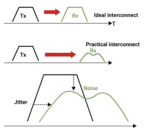
Figure 17. Jitter and noise in an eye diagram.
Time-domain reflectometry (TDR) can pinpoint where impedance mismatches occur and provide insights into the integrity of the transmission line, helping designers address issues such as signal reflections and losses. How it works:
- A TDR tester sends a signal into the device under test (DUT).
- It measures signal reflections as they pass through the transmission medium.
- Uniform impedance. If the conductor has uniform impedance and is properly terminated, there will be zero reflections.
- Impedance variations. Some incident signals will be reflected to the source.
- TDR compares the reflections with those generated by a standard impedance. It generates a graphical representation showing the reflected waveform’s timing, phase, and amplitude and accurately identifies the location and nature of electrical discontinuities.
Maintaining signal integrity in high-speed PCBs becomes more challenging in today’s fast-paced technological landscape. Unidentified signal integrity issues in a PCB design might question product accuracy and reliability. Consider these guidelines when designing the next high-speed board.
Amit Bahl is chief revenue officer at Sierra Circuits; This email address is being protected from spambots. You need JavaScript enabled to view it..


