Will a “universal” footprint work for various-sized passives?
This details the design of an LED constant-current driver PCB. I am trying to make this design as “universal” as possible. Described here are some of the features and reasons I created the layout as I did.
The outside dimensions of the PCB are 3.35" x 2.175". The PCB was designed so that all surface mount (SMT) parts are mounted on the topside (FIGURE 1) and through-hole (PTH) parts mounted on the bottom (FIGURE 2).
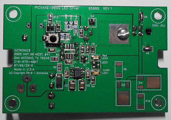
Figure 1. Topside of PCB showing SMT parts.
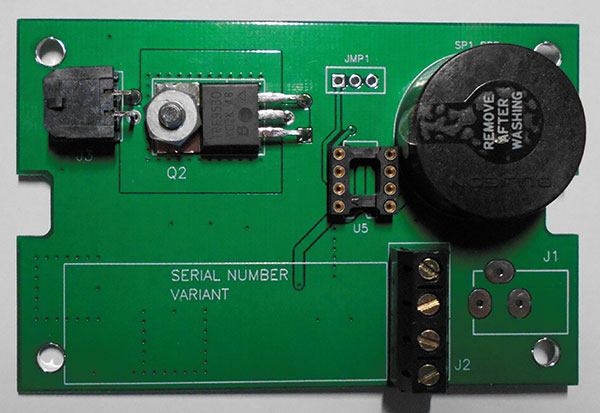
Figure 2. Bottom-side of PCB showing PTH parts.
The PCB was designed to fit into a single-gang plastic electrical box. A box this size permits easy use in home construction. (Not to mention that plastic boxes are inexpensive and readily available at any hardware store that carries electrical supplies.)
Dual power input connectors. Power input is in lower left corner of the PCB and aligns with the knockout in the electrical box. I used two connectors to permit multiple ways to provide power to the PCB.
The first method is using a 2mm barrel connector. This permits use of either a power brick or a 2mm barrel plug wired into the solar system’s wiring.
The second method is the terminal block that permits two wires to be wired to the PCB. Notice there are four connections on the terminal block (FIGURE 3). This is by design. Two can be used for power input, and two can be daisy-chained to another controller down the line.
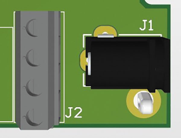
Figure 3. The four connections on the terminal block accommodate power input and connections to additional controllers.
While the present implementation of this design is used with a 12V input, it was designed to also be used with a 24V input with very few (if any) minor tweaks to the BoM.
Dual footprint for speakers. When designing the board, I saw two different speakers available (FIGURE 4). I was not sure which would make it to final production, and determined if one were out of stock, I could use the other. Both speakers have been shown to work well in the design.
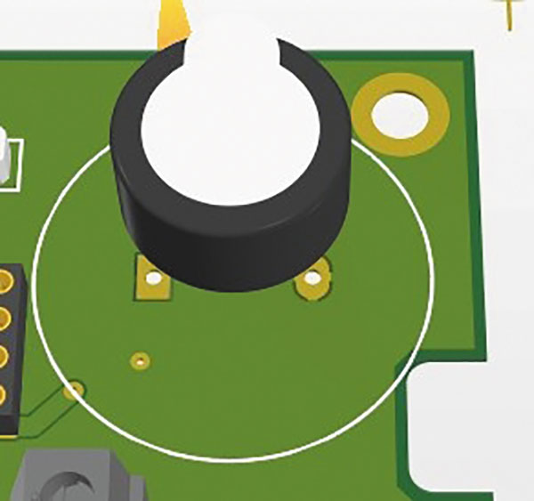
Figure 4. Speaker layout.
Dual footprint for microprocessor. Two versions of the microprocessor are available. The microprocessor is a PIC chip programmed with a version of Basic. It is easy to program using a serial umbilical that attaches to a 3-pin header on the PCB.
I placed the SMT version of the microprocessor on the topside of the PCB (FIGURE 5) and the PTH version on the bottom (FIGURE 6). Two microprocessor versions were included so the PTH version of the chip may be used during prototype development and the SMT version during production without a redesign of the PCB.
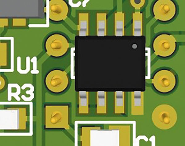
Figure 5. SMT microprocessor, used for production build.
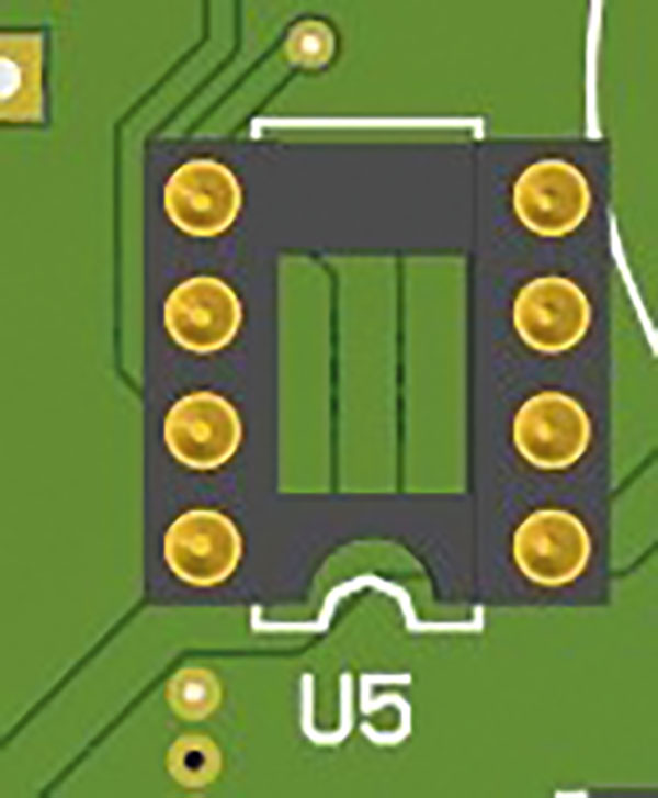
Figure 6. PTH microprocessor, used for the prototype.
Note the SMT version of the footprint is placed under the PTH version, but at a 90° rotation. I did this to allow easier routing of the traces.
‘Universal’ footprint. One of the footprints on the PCB is what I call a “universal” footprint (FIGURE 7). I designed a special footprint that permits the installation of any 0603, 0805, 1206 or 1210-sized resistor or capacitor. This was an experiment to see if I could do it. It turns out it works! Each pad is designed to have slots to prevent excess solder from the pads. The universal footprint is not needed on this PCB and will probably be removed in a future respin.
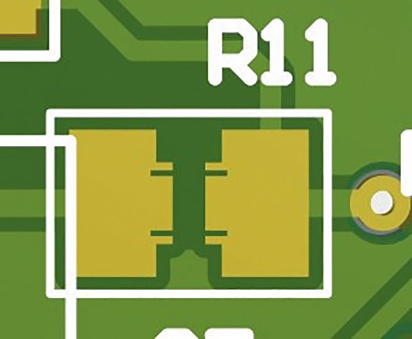
Figure 7. A “universal” footprint was designed to permit installation of any 0603 to 1210-sized resistor or capacitor. The slots prevent excess solder from the pads.
LED output connector. The LED output connector is in the upper right corner (FIGURE 8) and aligns with the other knockout in the electrical box. A different 4-pin connector was used, as it is readily available and there are mating 4-pin wiring harnesses available from the same vendor. Two different LED outputs are on this connector. One connects to the medium-to-high-current LED lighting, and the other output connects to the low-current LEDs that are on 24/7 and make up the night light.
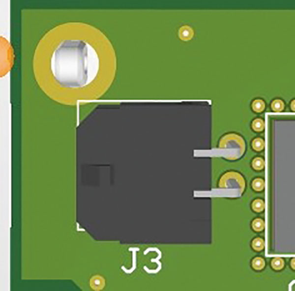
Figure 8. LED output connector.
FET switch. The FET for the LED switch is a PTH component mounted on the bottom side. It is an FET with a low rDS value and is rated at about 11A. This is more than enough current for the LED switch. I put copper around the FET and placed thermal vias around the perimeter of the FET, connecting the top copper to a heatsink on the bottom side, which should help dissipate heat.
Looking at what is available from vendors, many of my choices have now become unavailable or obsolete. The FET is not critical, other than it needs to be a P-FET with a Vds greater than 30V and capable of currents around 10A maximum. The lower the rDS, the better. The footprint needs to be a TO-252 to fit on the current layout.
Note how the three leads are bent (FIGURES 9 and 10). The center lead (source) is offset from the outer two pins. I did this to permit better separation of the leads.
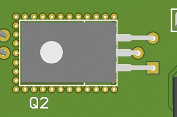
Figure 9. The FET’s center lead (source) is offset from the outer two pins to permit better separation of the leads.
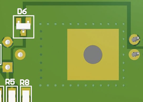
Figure 10. FET topside view.
Constant-current regulator (CCR). This brings me to the LED driver output design. I planned and designed the circuitry so that I do not have to use the CCR. I did this by adding a series resistor that can be used if CCRs are not populated. This also means I can drive the LEDs with currents that are limited only by what they can handle, within reason. The narrowest trace is 80 mils, which should be able to handle 2A to 3A of current. (I will make this wider in the next spin of the board.)
I expect to switch only 700mA using the CCR NSI45x series parts, which are currently not available or in limited supply. The two CCR footprints can be populated and run in parallel for increased output current.
The series of CCRs permit use of a current-setting resistor. Four part numbers can be used for this design (FIGURE 11). The first permits currents from 60mA to 100mA. The second permits currents from 90mA to 160mA. The third permits currents from 150mA to 350mA. The fourth does not permit an adjustable current and is internally set to 350mA.
Figure 11. Current-setting resistors come in four part numbers of varying currents.
With this in mind, the output current may be set from a variety of values of 60mA to 700mA (two 350mA parts in parallel).
Microprocessor details. The microprocessor, as mentioned, is an 8-pin PIC processor with a version of Basic burned into it. Using a free program, I can write a Basic program that controls various external devices that are attached.
Two of the pins are used for power and ground. Two more pins are used for serial communication and programming the device. This leaves four pins on the processor for various I/O functions.
This particular design (FIGURE 12) uses one pin for infrared input, one for a speaker output, one for a voltage-divider input and the last pin for the LED ON/OFF control.
Firmware. The Basic code for this design is not complex but performs the necessary functions. There are 2,048 bytes available in the PICAXE chip, and I am using 325B, which permits more features to be added.
When the board is first powered up, a welcome tune is played, with output to the speaker, to give an “I’m alive” indication. It then goes into a loop, waiting for an input signal from the IR input.
When it receives an IR input, it decodes the command. It can be an ON/OFF command or a command to set parameters within the device.
I also monitor the voltage on the voltage divider, and if it gets to 12.5V, the speaker emits a warning and the load (LED lighting) is disconnected to protect the battery.
One feature of this design is the OFF-Delay. This can be set to a value from 0 to 9. This equates to seconds before the LED lighting turns off. 0 equals Disabled, and 1 to 9 equals 1 to 9 seconds delay. While counting down to 0, the speaker emits a beep, giving an aural indication. I usually set the delay to 9. This feature allows the user to safely exit the room before the lights turn off.
Other features have been implemented as well but won’t be detailed here.
In the future I will incorporate a PWM feature for “dimming” to the LED output. This will add more than ON/OFF to the LEDs. This will be controlled using the IR remote and pressing the volume UP / DOWN. •
James Jackson, CID, is a senior PCB layout designer at Oztronics (oztronics-tech.com); This email address is being protected from spambots. You need JavaScript enabled to view it..


