Accounting for signal integrity and higher data rates for tomorrow’s PCBs.
5G is already here! It is already foreshadowing the capabilities of 4G Long-Term Evolution (LTE) wireless networks. So, the question does arise on the capability of the PCB industry to sustain the growing need for 5G wireless infrastructure. Demand for 5G will likely grow tenfold over the upcoming years, thus making it paramount for PCB manufacturers to embrace upcoming challenges. Moreover, 5G will likely drive demand for copper-clad material and add more value to the PCB industry. The ecology of the wireless access network device industry chain has changed greatly.
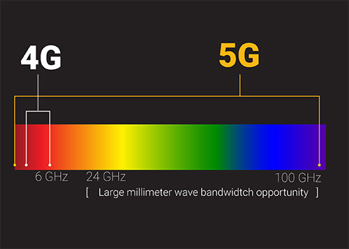
The exponential demand for 5G wireless networks is attributed to improved capacity and capability compared to 4G LTE systems. 5G wireless technology offers wider channel bandwidths, high-end antennas and modulation technologies. However, the 5G wireless infrastructure will operate on higher carrier frequencies in addition with mmWave (millimeter wave) frequencies. Thus, it becomes essential to achieve systems and circuits that can sustain higher frequencies than current 2.6GHz 4G LTE wireless networks.
Several standards have been implemented for 5G wireless networks to achieve data rates up to 10Gb/s and beyond with low latency. Higher frequencies are required to provide low latency in comparison with traditional wireless communication systems. The rising approval rating by the US Federal Communications Commission (FCC) for use of frequency bands at 28, 37 and 39GHz for 5G will likely fuel adoption of 5G systems over the coming years.
Deployment of 5G RF, along with Massive MIMO (large-scale antenna array) technology, has generated substantial buzz. The number of 5G base stations has increased swiftly over the past few years compared to 4G stations, particularly in China, the US and Japan. This will likely generate higher revenue for the PCB industry chain, as the value of high-frequency PCB/copper clad material for 5G base station antennas is rising faster than that of 4G. Also, the 5G network infrastructure can carry more broadband flow.

Figure 1. Bandwidth spectrum of 4G and 5G.
Key Challenges for PCB Manufacturers
5G wireless infrastructure offers unified connectivity solutions. This allows mesh encompassing of people, autonomous vehicles, smart connected devices and industrial machines. Rising adoption of the 5G wireless infrastructure will help improve public infrastructure in the forthcoming years. The real-time system requires faster download speeds and lower latency for sustained communication signal, thus permitting better responsiveness.
Growing demand for 5G systems, for the seamlessness of augmented reality and virtual reality (AR and VR) experiences, will further escalate the need for high-end PCBs. The precision of machine-to-machine (M2M) communication is dependent on the performance of higher frequency mmWave systems. Furthermore, adoption of ultra-low-latency 5G wireless systems will allow improved transportation with the help of faster connectivity rates in autonomous vehicles and roadway/airway sensors. This will directly improve passenger safety, as vehicle response time will be in milliseconds. Thus, it becomes paramount for PCB manufacturers to provide boards with all the above capabilities.
The concerns for PCB manufacturers include relatively smaller margin for error, the risk of system malfunction and communication failure. The risk associated with
communication increases exponentially with the addition of new electronic devices connected to the network.
Hence, PCB manufacturers must maintain higher standards to ensure performance and quality during real-time 5G communication. Various technologies and processes are developed and implemented to address these challenges. Several manufacturers are reiterating their production processes to build a sustainable manufacturing system. This not only enhances quality assurance but also boosts production efficiency.
Higher frequencies. Do we need to move beyond RF and microwave frequency systems? Will EHF (extremely high frequency) spectrum help achieve our needs? We must answer a few questions before moving forward. Are we capable enough to go further with higher frequencies, 5G and ADAS (advanced driver assistance systems) radar?
We have eagerly awaited a brighter tomorrow with 5G systems. The wait is over. Existing cellular networks provide download speeds of somewhere in the 10s of megabits per second, with latencies around 70ms. 5G systems are capable of operating beyond 10Gbps download speeds with latencies under 10ms, as they work within the EHF spectrum. This also gives far better data rates, along with wider frequency bandwidths and lower latencies. To attain these data rates, however, PCB manufacturers must implement substantial changes.
Material selection. Higher frequency mmWave systems are increasingly adopted for 5G communication systems. The design and selection of PCB materials for mmWave systems merits substantial consideration. These materials are specifically selected to obtain higher frequencies, taking into consideration PCB effects, such as copper surface roughness, Dk variations and thermal dissipation. Other factors, such as passive intermodulation, coefficient of thermal expansion (CTE), thickness variations and EMC/EMI are also taken into account.
PCB manufacturers must understand the various trade-offs of dielectric PCB materials. The key criteria for PCB material selection include lower Dk, copper roughness and thickness variations. These design considerations are essential to avoid costly iterations and achieve accurate models and simulations. Here are some critical parameters:
- Lower Dk. A critical parameter to consider before selecting any PCB material. Material selection becomes critical for quality performance of PCBs, as it should meet requirements of EHF systems. For EHF systems, PCB material with the lowest Dk is needed in order to to avoid any Dk losses. For the selected mmWaves, use materials with the absolute lowest Dk. Dk losses increase proportionally with frequency. That means a moderately low Dk is no longer acceptable.
- Minimal amount of solder mask. It is highly important to check the moisture absorption capacity of the solder mask. Typically, solder mask has a higher water absorption capacity compared to the substrate. This has a significant impact, as the Dk of water is almost 70. This will likely induce higher losses in the mmWave circuit. Thus, it is preferable to use as little solder mask as possible during PCB prototyping.
- Very smooth copper. Higher quality copper is typically required for a smoother copper surface on the board. It has been recorded that skin depth for current at higher frequencies is very shallow, greatly increasing overall losses. Rough copper will lead to increasing resistive losses due to the increased current path. Select smooth copper over rough copper.
TABLE 1 shows some PCB materials highly preferred by PCB manufacturers.
Table 1. Typical 5G Materials

Signal integrity. Higher frequencies pose major challenges for PCB manufacturers. One common challenge faced during manufacturing includes the shrinking form factors of electronic devices. High-density interconnects (HDI) are specifically designed in PCB layers that require thinner traces to maximize I/O. This will also decrease the overall system size, which will lead to finer lines. This can further cause signal degradation. The physical parameters of line traces change along the top and bottom from the desired design, leading to further losses.
These losses impact RF signal transmission, which is delayed by milliseconds. When signals are not synchronized, this can lead to cascading issues across the signal chain. At higher frequencies, signal integrity relies strictly on impedance control due to the narrow geometries of the trace, which directly affects the line’s cross-section dimension, shape, line and space width, and dielectric material.
Trapezoidal cross-sections are commonly formed using conventional subtractive etching process. These cross-sections are formed along traces, causing myriad impedance anomalies. Deployment of advanced semi-additive processes (mSAP) will solve the issue and enable traces to be formed with greater precision. This also yields a line with straighter walls, which will further enable predictable impedance control.
AOI. Every PCB manufacturer must build up AOI capabilities, including pattern inspection or multi-image verification. This will likely provide fabricators with tools to determine significant process inefficiencies. Adoption of these solutions and tools limits space on the manufacturing floor. The absence of AOI, however, can halt the manufacturing process, where panel sampling is required during manual microscopic measurement. Recent advancement in AOI capabilities can save time and money for PCB manufacturers and offer several growth prospects during the upcoming years.
Deployment of newer automated inspection methods to determine top and bottom trace conduction, along with increased adoption of 2-D metrology technology, will help overcome 5G challenges. Use of these technologies permits optimal line shape and width, thus enhancing the overall impedance control in high-frequency 5G systems. Increased adoption of automated inspection methods also allows consistent performance at high throughput rates and high sampling rates.
Recent Advancements in 5G Hardware
In the past few years, several telecom companies and manufacturers have raced to achieve supremacy in 5G. Development of mmWave systems, mMIMO and a variety of software and hardware are considered stepping stones for a number of these businesses. Several technologies have been developed and implemented in accordance with the upcoming 3GPP Release 15. These technologies are aligned with regular software updates, thus meeting the final 5G Phase 1 specification and future requirements.
Some leading hardware manufacturers and telecommunication companies are making substantial efforts for 5G trials and deployments. Over the next five years, we will likely witness non-standalone 5G, and new 5G radio technology implemented with the finalized specifications. The adaptability of boards will become a major topic for discussion among industry experts and directly impact the commercialization of 5G. This will also hamper the likelihood of future 5G specifications adjusting to the findings of early trials and deployments.
Pankaj Shrotre is a content writer at Sierra Circuits (protoexpress.com).


