IoT designs operate in multiple modes, and often must fit predetermined form factors.
Expectations for growth of the Internet of Things (IoT) seem to increase almost daily. Worldwide spending on IoT is forecast to reach $772.5 billion in 2018, an increase of 14.6% over the $674 billion spent in 2017.1 Annual revenues could exceed $450 billion by 2020 for IoT vendors selling hardware, software and comprehensive solutions.2 In 2018 the number of IoT connected devices will surpass the number of mobile devices.3 And by 2020 there will be 3.4 connected devices per person.4
In today’s marketplace, designing electronic products with IoT capabilities is no longer optional; it is a requirement to compete. IoT technology not only opens up numerous new product categories of electronic devices, it drives innovators to rethink the ways consumers interact with traditional tech-less products. From makers to startup companies and beyond, the opportunities to invent new tech devices and reinvent existing products with IoT capabilities are seemingly endless (FIGURE 1).
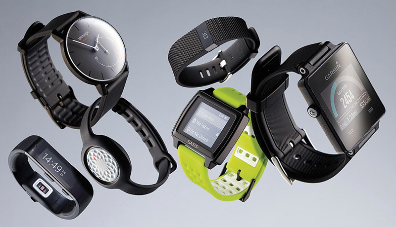
Figure 1. Examples of IoT-capable wearables.
The ecosystem of IoT-enabled devices is growing faster than ever, connecting the world of objects, systems and people with products that connect users to users, to other devices, and even to manufacturers. To consumers, IoT devices look sleek and simple, but they are comprised of a distinct set of components, physical interfaces, PCBs and circuitry that presents unique design and layout challenges. Modern IoT designs require a PCB design environment with advanced functionality that includes pre- and post-layout simulation, layout constraint management, verification, and more.
This article describes critical areas that must be considered when designing PCBs for the Internet of Things.
IoT Domains
Analog (A) and digital (D). Analog-to-digital converters are used in IoT designs to process, store or transport virtually any analog signal in digital form to a microprocessor. These converters are most often referred to as A-to-D (A/D), D-to-A (D/A), and ADC (analog-to-digital converter). The ADC is a mixed-signal device that provides an output that digitally represents the input voltage or current level. The key advantage of analog is that it offers an infinite number of representations, while digital has a finite number of possible representations. Converting from the analog world to the digital world enables use of electronics to interface with the analog world around us.
MEMS (micro-electro-mechanical systems). MEMS are miniature sensors and actuators and are now commonplace in many of today’s IoT designs. MEMS sensors gather information from their surroundings, while actuators execute given commands. From fitness trackers that detect steps to smartphone sensing when the phone is tilted and rotated, MEMS are key components in IoT design.
RF (radio frequency). A radio module connects the IoT device to the cloud via Wi-Fi, Bluetooth, or custom protocols. Multiple factors, including application needs, technology constraints and different hardware and software integration requirements, must be considered for wireless connectivity. Understanding the IoT product’s power consumption, range, connectivity and throughput is critical to meeting each device’s wireless technology requirements.
Form and fit. A driving requirement for the design of many mass-consumer, particularly human-interface, IoT devices is the form factor. If a fitness tracker is not light, comfortable, or even fashionable, or if a smartwatch is too bulky, or an IoT door lockset doesn’t fit in aesthetically, the product is unlikely to ever get off the ground. IoT devices are typically developed in one of two ways. The first is to explore, design, and develop the product with a proof-of-concept prototype. Once the prototype is proven, market demand can be quantified by investigating whether the device can be packaged in a consumer-friendly form factor and meet the consumer price-point requirement. In other words, the form factor follows the product development. The second development process is more typical for an established company. In this case, the form factor precedes product development. For example, for an IoT wearable, size and weight drive the product shape and overall look and feel. Once the form factor is established, the PCB is then developed to conform to the predetermined enclosure.
IoT components. An important step for IoT devices is researching and selecting all of the proper components. Part selection for analog/mixed-signal ICs, D/A-A/D converters, sensors, actuators, MEMS, and radio modules is critical with regard to both functionality and cost (FIGURE 2). IoT products often have miniaturized components, including LEDs, displays, cameras, microphones and speakers. Additionally, physical interface components such as buttons, switches, touch sensors and charging ports are typical. IoT devices may even contain reed sensors, fingerprint detectors, force sensing resistors (FSR) and flexibility sensors. Human interface devices (HID) like smartphones and compact wearables that house batteries with wired or wireless charging are low power and highly efficient, while other IoT-enabled devices that have been historically low-tech such as doorbells and thermostats make use of existing electrical wiring for power.
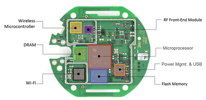
Figure 2. Typical components in IoT design (example: Nest thermostat).
Capturing IoT design intent. Once selection of critical IoT components is completed, and the schematic symbols have been created in the library, the next step is to define the connections between the components in a schematic diagram. To ensure design efficiency and productivity, schematic creation should be integrated with component management to properly source components and manage costs. Direct access to analog/mixed-signal circuit analysis and pre-layout signal integrity analysis from within the schematic design environment is critical to ensuring the design’s physical characteristic requirements are achieved.
Simulation, validation, power and memory. IoT designs contain analog and mixed-signal (AMS) circuits. The high performance of AMS circuits is achieved through model-based AMS design, simulation, and analysis for mixed technology. This can include time domain and frequency domain analyses, parametric sweep, sensitivity, Monte Carlo, and worst-case investigations. The behavioral verification, scenario exploration, and component optimization of an AMS circuit are critical to ensuring the design intent, performance, and reliability of IoT designs.
IoT designs are unique in that they typically operate in multiple modes, such as standby, transmit/receive, active sensing, recharging, etc. As such, functional verification of each mode, and from mode to mode, must be specified and verified. For example, transistor-level simulation is required to verify that a built-in A-to-D converter operates correctly in a specified temperature range. Performing pre-layout simulation and planning for post-layout verification is critical for ensuring the design meets all the product’s functional requirements.
Many of today’s most popular IoT devices are compact wearables. They are small, lightweight, and must be extremely power-efficient. Power consumption must adjust from mode to mode to preserve battery life, which, in turn, reduces the time between charging. To prevent product malfunction or failure caused by voltage loss on critical supply nets, it’s important to analyze power integrity during layout. Unexpected or unpredictable circuit behavior can also be caused by power-delivery issues. To ensure power going to the ICs is clean and efficient, it’s important to find and resolve areas of excessive current density early in the product creation process.
IoT products use modern microprocessors that connect to DRAM and flash memory. To take into account board-level effects such as lossy transmission lines, reflections, impedance changes, via effects, ISI, crosstalk, timing delays and more, detailed simulations are necessary to provide a comprehensive view of the memory interface. The ability to accurately constrain and route memory connections is essential to reducing design time and debug cycles of DDR-based designs. By utilizing PCB layout functionality that includes advanced constraint management and advanced DDR routing, designers can quickly and accurately route high-speed, high-bandwidth traces.
PCB Layout
The form factor for IoT products is typically designed using a 3-D mechanical CAD tool. Being able to visualize the board in its enclosure in 3-D prior to routing traces or pouring planes is essential for ensuring the design will meet all of the product’s physical requirements. In addition to the PCB outline, other factors, including the product’s use environment and flexibility, must be taken into consideration. Here are some of those factors:
- Component placement. Once the IoT schematic design is complete and board outline (including fixed physical interface component locations, mounting holes, cutouts, etc.) has been imported into the layout environment, component placement should be quick and easy. The ability to place components in 2-D or 3-D, while ensuring the placement meets the design constraints, reduces design time and avoids violations.
- Constraint management. Since components are often referred to as the building blocks for the PCB design, think of the connections between these building blocks as the mortar. Using integrated constraint management to propagate predefined electrical constraints throughout the design flow lets the design team control net classes and groups, define pin pairs, and more. Hierarchical rules nest constraints for more efficient route control, ensure that routes meet high-speed performance rules, and enable engineers to define high-speed rules for matched lengths, differential pairs, max/min lengths and more.
- 2-D/3-D layout. When designing an IoT product with tight form-factor constraints and a complex assembly procedure, having the ability to lay out and explore the design within a detailed 3-D physical layout environment offers a huge advantage. With photorealistic 3-D visualization during placement and dynamic design rule checking (DRC), the team can ensure the layout is correct by construction. Accurate STEP models of components provide a view of the end product that ensures the fit and clearances meet product specifications. Additionally, the ability to import the IoT product’s mechanical enclosure into the 3-D view gives the designer a photorealistic view of the final assembly to ensure fit and avoid conflicts.
- Rigid-flex circuits. Flex and rigid-flex PCBs are now found in all types of electronics products and are frequently required for IoT designs (FIGURE 3). 3-D verification ensures bends are in the right position, and components do not interfere with folding. Managing flex bends, flex routing and plane shape fills, etc., is critical for these designs. The ability to visualize IoT designs with rigid-flex early and throughout the design phase can prevent costly redesigns. Furthermore, exporting the rigid-flex design as a 3-D solid model to MCAD promotes efficient bidirectional collaboration between ECAD and MCAD domains to ensure manufacturing (DfM) and assembly (DfA) issues are avoided.
- Testing. Many IoT products are low-power and require test platforms that can adapt quickly to new technologies. Four key testing parameters for wireless IoT products are range, battery life, interoperability, and response time. Devices that use Bluetooth technology, for example, will have shorter ranges than those that use Wi-Fi technology. For battery-powered IoT devices, it’s necessary to measure the power consumption of the device in realistic scenarios to ensure they have sufficient battery life throughout multiple modes.
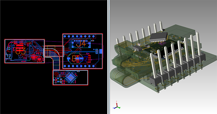
Figure 3. Rigid-flex layout in 2-D and 3-D.
Manufacturing and assembly. Ensuring IoT devices are designed for manufacturing and assembly should be considered throughout the product design flow. DfT (design for test), for example, can ensure testability of the design from a bare-board perspective to identify shorts and other manufacturing defects. Similarly, performing DfMA (design for manufacturability and assembly) analysis can identify issues such as resist slivers and unintended copper exposed by solder mask, so they can be corrected prior to fabrication.
Summary
Designing PCBs for the Internet of Things requires some unique planning and consideration, including:
- Proper selection and utilization of IoT-specific components.
- Focus on simulation, validation, power and memory requirements.
- Visualizing the products’ flexibility and use environment during PCB layout (product-level design).
- Planning for efficient manufacturing and assembly.
- In the end, proper attention to detail can ensure companies developing IoT-enabled products not only compete but thrive, whether they are inventing new devices or reinventing traditionally low-tech products.
References
1. International Data Corp. press release, Dec. 7, 2017.
2. Ann Bosche, David Crawford, Darren Jackson, Michael Schallehn and Paul Smith, “How Providers Can Succeed in the Internet of Things,” Bain & Co., 2016.
3. Ericsson Mobility Report, Internet of Things Forecast, November 2017.
4. Cisco Visual Networking Index (VNI) Complete Forecast for 2015 to 2020, June 2016.
John McMillan is marketing program manager for Mentor, a Siemens business (mentor.com); This email address is being protected from spambots. You need JavaScript enabled to view it.. Craig Armenti is PCB marketing engineer for the Board Systems Division of Mentor; This email address is being protected from spambots. You need JavaScript enabled to view it..


