For those new to electromagnetic compatibility, I’m not about to get into the physics of electromagnetic theory, but will jump straight to the electronics design challenges and then move on to provide tips that you can get on with straight away to overcome these.
If you do want to find out more about the physical interaction between the electrically charged particles that is known as electromagnetism, Wikipedia does a sufficient job of explaining it.
You’ll already be well aware that EMC compliance is a necessary condition for releasing products to market. There’s national and international bodies such as the IEC and FCC that define limits on how much a device is permitted to produce, and the how stringent these are vary according to industry.
Definitions
While I’m not going to indulge you in the world of physics, some basic definitions are essential before we move on.
- Electromagnetic compatibility (EMC) is the ability of a product to function in its environment without introducing electromagnetic disturbance. So the product must:
- Tolerate a specified degree of interference.
- Not generate more than a specified amount of interference.
- Be self-compatible.
EMC is the control of EMI as described below:
- Electromagnetic interference (EMI) is disturbance that affects an electrical circuit due to either electromagnetic induction or electromagnetic radiation.
- Electromagnetic noise is the interference we are talking about above, which is produced as a result of rapid current and voltage changes.
EMC Design Challenges
We don’t need to talk about the electromagnetic spectrum to appreciate that the difficulties surrounding EMC stem from two areas: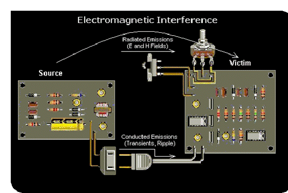
- Emissions. This is the unwanted energy created by components or traces that can interfere with other components and traces, etc. The designer is focused on minimizing or blocking this. They might be just getting on and doing their business, but think of all the components they are messing with around them.
- Susceptibility. This is the component or trace that is the victim of the unwanted energy (noise) from the emission released above. This is the regular component just doing its job, them wham, it is bombarded with electromagnetic interference that causes all kinds of havoc. The designer might want to move these components or find ways of toughening them up so they aren’t affected.
The upshot here to ensuring compatibility is about addressing both the (selfish) emission releasers and the (unsuspecting) victim of the releases. Think of someone playing loud music on a train. You might get them to turn their music down so it is not being so intrusive ("Hey man, can you turn it down please?"); you could get used to the loud music ("OK, so this track is not so bad"), or perhaps you could wear ear plugs or ear defenders ("I will not let this awful music ruin my commute this morning.").
Four Steps to Ensure Acceptable EMC
We all like a set of easy steps don’t we? Here’s four to get you started toward EMC heaven.
- Characterize the threats – understand what the potential is.
- Review the standards for emission and susceptibility levels – how does the threat apply within these?
- Design for compliance – make sure you keep compliance requirements in mind throughout the design process.
- Analyze and test for compliance – use your design tool prior to fabrication. Make sure it can:
- Perform appropriate rule checks for critical wiring and parts.
- Ensure rule checks are well documented (explain and advise on correction).
- Support thresholds and allow weightings.
- Allow both quick analysis and in-depth analysis.
EMC Quick Design Tips
Now let’s get to the technical detail, here’s some tips to start implementing straight away.
- Place decoupling capacitors as close to the power pins of ICs as possible. If wiring rather than using vias, make sure the wiring is as short as possible.
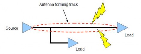
- With clock wiring, keep as short as possible to avoid potential antenna.
- Eliminate isolated copper areas to avoid potential antennas. Connect any isolated copper areas to ground.
- When working with power and ground nets, minimize the loop areas as they can act as receiving antenna for external noise.
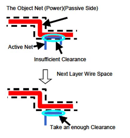
- Monitor the proximity of wiring which can easily generate noise to wiring to those that can easily receive noise. Insufficient clearance can result in “crosstalk” (when one signal creates an undesired effect on another signal).
CRAIG ARMENTI is an application engineer at Zuken USA (zuken.com). He has been in electronics engineering since 2000 with Motorola and Blackberry, among others, and is a past speaker at PCB West; This email address is being protected from spambots. You need JavaScript enabled to view it..


