Are pad designs for flex circuits different from those for rigid?
Recently I have seen designs that on the surface looked like garden-variety flex assemblies, but on closer examination showed troubling pad design. It was clear these designs would cause difficulties down the assembly line. Design rule check (DRC) programs do a fine job of locating potential routing errors, missing pads, and improper fillets, but can do little to actually review the design with an eye toward consistent, error-free assembly. I will go out on a limb and suggest that nearly all assembly issues begin with poor pad design!
When a prototype lot of, say, 20 pieces is run, final yields are likely far down the list of concerns. Thanks to DfM and DRC procedures, we have a good idea that our prototype will fall within the manufacturable range. If final assembly yield hits 95%, we may not even give it a second thought. But what happens when that small prototype run is signed off and production entered without a thorough review of what our assembly process actually yielded? Ninety-five percent is simply not acceptable. If we wish to build hundreds of thousands, or even millions, of units we need to verify we are “production proven” before the first production lot is run.
Each component supplier will provide a recommended pad pattern for use on our PCB/flex. Issues arise when the component manufacturer’s pad design may not be optimal for a given application. Pad libraries are only the starting point. The designer needs to look at that component and consider what may happen to it during the reflow process.
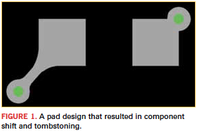
Surface tension of the molten solder helps hold or guide a component into its final position during reflow. As solder cools, inconsistencies within the artwork pad pattern can cause the component to shift. The smaller and lighter the component the more critical this becomes. Pad design must not only be consistent from like component to like component, it must be consistent within the individual pad pattern itself. Figure 1 shows one real-world example where not only did the component shift in reflow, it also tombstoned. Both were common issues with this one component location; identical components nearby had no such trouble. The root defect cause was identified as differing via connection strategies between the two pads, which caused slightly different heating and cooling rates during preheat and reflow. As the solder cooled it “pulled” the component from each end at different rates, causing skew. In some cases solder would wet at slightly different times on opposite pads. When this happens with a small component, one end will rise off the pad as it is pulled by the surface tension of the molten solder.

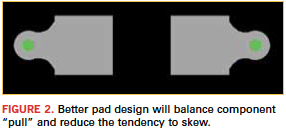
While there are several fixes for this (via-in-pad is a viable option, though at an increased cost), Figure 2 shows a simple suggestion. Here it clearly shows that the pad design will provide a consistent “pull” on both ends of the component. Identical pads and connection methods ensure an aligned component and good solder joint.

Large and/or heavy components such as large BGAs are less prone to movement and therefore less susceptible to component drift during reflow. On the other hand, small and light components such as 0201s are very sensitive to pad size and shape. When we lay out pads for these components we need to consider the impact of several factors:
- Placement equipment tolerance (should be +/-0.0015").
- Solder paste volume.
- Stencil thickness.
- Pad size, shape, location.
- “Auxiliary” conductors, vias, etch pattern.
One last reminder: All flex must go through prebake prior to any SMT/reflow process. A key difference between flex and rigid FR-4 is flex circuits are made from polyimide film. Polyimide is hydroscopic and can absorb close to 3% of its weight in water when directly immersed. Exposure to humid air is not nearly as dramatic, but the moisture can cause real havoc if not driven out prior to reflow. Prebake should be performed at 250˚F (120˚C) for 1 to 6 hr., depending on circuit thickness or material type. Your times may vary. Important: You must process the boards shortly after pre-bake or store the panels in a “dry box.” Try to process all boards, rigid or flex, within an hour or less from pre-bake.
Mark Verbrugge is a field applications engineer at PICA Manufacturing Solutions (picasales.com); This email address is being protected from spambots. You need JavaScript enabled to view it.. He and co-“Flexpert” Mark Finstad (This email address is being protected from spambots. You need JavaScript enabled to view it.) welcome your questions.


