 To land the job you want, it pays to be grounded and groomable.
Starting a new job is a big deal even if you're not leaving your current company. It's a commitment to learn the ropes while being humble and deferring to those in the know. In the field of PCB layout, a lateral move is often as good as moving up if the move expands your skill set in a way that helps your long-term goals.
Long-term goals should be about more than money. What is your dream company? What is the role that would keep you engaged or become a step toward the top rung of your personal career ladder? My niche is in wireless. Once that die was cast, the industry kept pulling me back into its orbit. It is nearly always that the employer initiates the contact for a new opportunity.
GoPro is no exception, with lots of analog work in capturing audio and video from the physical world while streaming geo-located image data over Wi-Fi. Meanwhile, the in-house graphics chip is as complex as anything I've seen on VR/AR headsets, laptops or smartphones.
Like most other handheld products, size, performance and battery life are the competing interests. The company wisely gives us cameras and encourages us to put them through their paces. It gets packed along for my morning walk out by the bay. Then, when something isn't responding as it should, I can raise the issue with the development team.
Google did the same thing with its products but gave us the goods well before they were launched. That could be the main difference between a small company and a mega-corp. It had to help that the marketing department could carry the company on its own with all the R&D you can imagine. The hard part is spending that much money wisely.
The "G-Chips" team sure gave me a lot of IC package footprints for fan-out studies. After enough of them, you get a feel for what type of stack-up it would take based on pin pitch and quantity. A lot of PCB technology is driven by the available devices. Chip companies compete to fill the socket and their top factors are aligned with the OEMs in size, performance and power efficiency.

Figure 1. Various devices share a board with shielding separating functions to improve coexistence.
Setting up your career path by focusing your résumé. Whatever you are doing now should reflect what you want to be doing down the line. After a little self-examination, rewrite your résumé with a focus on what you want to do next rather than including every major accomplishment. Be especially vigilant to minimize anything major you don't really want to keep doing. Whatever you mention has a chance of attracting a recruiter who wants to fill a spot. By saying exactly what you've done, you're asking for more of the same.
People who write job descriptions are throwing out a common list of buzzwords. You can expect high-speed digital or high-frequency analog to be among the requirements. Those technologies will be implemented differently depending on the specific application.
Thick telecom backplanes are a different world to consumer goods, where back-drilling is unlikely. Whatever skill is common to the industry will be on the list. List the things you want to do in hopes of finding an outfit that wants you to do just that. The hiring manager wants the designer to fit the description like a key in a lock. For better or worse, your résumé buzzwords are that key.
Chip companies come in two sizes, tiny and internationally known market leaders in their particular segment. Getting started in a startup is risky. It can take months after tape-out to get the first silicon back from the foundry. The ceramic substrates take about the same lead time. The company's funding isn't going to be enough for a second spin, so the first pass is a moonshot. "Do, or do not. There is no 'try.' "
While the venture might not work out financially, you get to keep everything you learned there. Numerous segments specialize in different core functions. When looking for talent, they place a premium on skills that fit their niche. A generalist PCB designer can walk right into most situations, but the hiring team has to be convinced it is a low-risk choice with at least some crossover between their requirements and your accomplishments.
In a tight labor market, that effort can expand to finding a groomable candidate in an adjacent field. I didn't know anything about 40GB/s optical transponders, but I was well grounded in RF and had worked with lasers in the past, so a startup took a flier on me. I packed up my one-person service bureau and hopped on the dot-com boom.
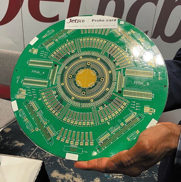
Figure 2. Probe cards may be the ultimate fan-out exercise. You better like round boards if you want to be happy working with a chip team.
High-performance substrates: AIN and LTCC. I landed a job in a company with in-house chips and they cut me loose with the IC package design software. It is not hard to learn if you already know the PCB tools. The real learning curve came in the form of the details around the LTCC (low-temperature co-fired ceramic) materials. There was no room for negotiation. Until then, I considered 25.4µm and 25µm to be essentially the same thing.
It all starts with the ceramic in the form of tape in the so-called green state – prior to firing. During the green state, holes are punched into the tape, which are then filled with a metallic paste. Then, the circuit pattern is applied prior to going into the kiln. While being fired in the kiln, the parts shrink by a controlled percentage, about 15% in the z-axis, a bit less in the x and y dimensions.
The via fill material doesn't shrink by that same percentage. For that reason, we limit the number of layers that a via could traverse before sidestepping with a pair of vias on one layer to hand off the signal to continue on its vertical path. The bottom line here is that a complete stack of "microvias" through the entire LTCC stack of, let's say, 21 layers would lead to a defect they call posting. It would not lead to a flat surface, which is useful for a seal ring or a solder joint.
This via-posting avoidance technique is one of many quirks involved with providing a carrier for the silicon. I use the word "silicon" to describe the chip, but other materials will come into play, some of them seriously toxic. A lot goes on that you don't get to see in a chip company unless you put on a "bunny suit" that covers you and your tiny dust particles. I can already tell I wouldn't want a job inside the foundry.
The ebb and flow of a chip provider. Supporting a chip team can be somewhat seasonal where a pulse of work is followed by some downtime. Your life will revolve around the chip tape-out period. Everything that could be anticipated is covered in the initial printed circuit board revision. The team must be able to measure performance so it can be fine-tuned.
The second revision is informed by the reality of the situation. There can be flaws among the nearly uncountable transistor gates on a device. Imagine doing a revision on a board without moving a via or adding or removing one. We can sometimes revise the chip on a shorter lead time if it is just a metal spin done that way at the device level.
Often, there is no easy fix on the die, so our job is to find patches for those bugs and make the device whole before it goes out into the world. We can spin out a PCB quicker than a new chip even if the original punch sequence is reused. This is all-hands-on-deck time. Be a hero. Save the product launch. Save the company in some cases. In any case, look forward to a successful landing. That's what matters in the chip game. •
John Burkhert Jr. is a career PCB designer experienced in military, telecom, consumer hardware and, lately, the automotive industry.
Originally, he was an RF specialist but is compelled to flip the bit now and then to fill the need for high-speed digital design. He enjoys playing bass and racing bikes when he’s not writing about or performing PCB layout. His column is produced by Cadence Design Systems and runs monthly.


