What to do when the trace doesn’t act as an “ideal” connection.
If you’re like me, you may have taken a few physics courses, and upon successful completion of those courses, said to yourself, “That was fun, but as an electrical engineer, when would I ever be analyzing the projectile curve of a catapult launch?” While understanding and applying physics in electronics design might not be as exciting as catapult launching an object to land in an exact location (FIGURE 1), it is just as – if not more – important to consider when creating functional printed circuit boards (PCBs).
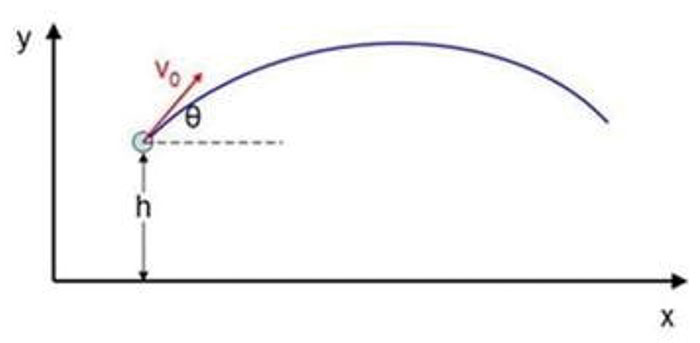
Figure 1. Catapult projectile motion.
Modern electronics almost always require design decisions to account for possible signal integrity (SI) complications. Here’s why: simple circuit analysis generally assumes “ideal” connections between components. That is, every part performs as if it has ideal electrical connections to other components. Imagine the difference between launching an object with your catapult into a perfect vacuum, versus in a field on a windy day. The properties of the real-world environment (in this case, wind and drag) will greatly influence the behavior of the object’s trajectory compared to launching in a perfect vacuum. This same idea must also be applied to the behavior of electronics.
At low frequencies and short distances, it can “mostly” be assumed a PCB trace will act as an ideal connection (i.e., a zero-ohm resistor). In other words, the physical trace itself does not have inherent resistance, capacitance or inductance influencing its behavior. Unfortunately, this only applies to circuits operating at a low-enough frequency over a short enough distance. When the length of the signal trace becomes relatively long in comparison to the frequency of the signal, the signal trace must then be considered a transmission line. When signal frequencies reach a high enough speed, as is the case with almost all electronics systems today, even a very short PCB trace is still a transmission line. Because of a transmission line’s high operating frequency, the AC (frequency response) electrical characteristics create an inherent resistance, capacitance and inductance on the trace, which are collectively known as the characteristic impedance Zo.
Reflections. Say you fill a rectangular tub with water, then push the water from one end of the tub toward the other, creating a “wave.” As soon as that generated wave reaches the opposite edge of the tub, some or all of it will be “reflected” back toward you. Now, imagine that rectangular tub was infinitely long. When you generate the wave (ignoring other external resistive factors), none of it can be reflected, because the tub goes on forever. This is the same concept as impedance matching. When the load impedance on a line is the same as the line’s characteristic impedance, it is effectively like having an infinitely long transmission line. The load will absorb all the energy, preventing any reflections. Now, imagine the real tub: when the wave reaches the end of the tub, some of it reflects toward the source. This corresponds to an electrical circuit with an impedance mismatch at the end of the transmission line. The differing impedance values cause part of the signal wave to be reflected to the source from the load. If the source impedance is also not matched to the line, this reflected wave will continue to travel back and forth between source and load, getting partially absorbed each time, until all its energy is depleted. When reflections are present on a line, they can significantly disrupt the original signal, leading to a host of data complications.
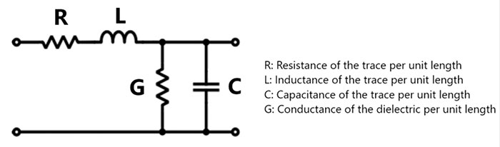
Figure 2. The electrical characteristics that make up characteristic impedance.
Crosstalk. To better explain crosstalk, I’ll start with the question what is a capacitor? Capacitors generally consist of two parallel metal plates separated by a nonconductive dielectric material. When voltage is applied over the metal plates, it will produce an electric field. Now, think about closely spaced parallel electrical traces on a PCB. The conductive traces, and the narrow space between them, will produce a small capacitance, especially at higher speeds and closer proximity. This “mutual capacitance” can be responsible for the transfer of energy from one trace onto other nearby traces; i.e., coupling. Additionally, the inherent inductance present on a PCB trace at high speeds creates a magnetic field, which can induce a smaller, opposite magnetic field on closely placed parallel traces. This energy coupled between traces as a result of mutual capacitance and mutual inductance is known as crosstalk. Crosstalk can create numerous undesired effects on the victim traces, so minimizing its presence is necessary. Some techniques used for this include leaving wide spaces between nets, reducing the length of parallel trace segments as much as possible, proper placement of ground planes to transmission lines, and using differential pairs, when necessary.
Reflections and crosstalk are just a couple of the SI complications associated with the real-world physical properties on high-speed signals. Taking all these potential problems into account when designing a PCB is no small task, especially with the industry demand for highly complicated, densely packed circuitry. As you can imagine, these mistakes are easily made and, unfortunately, can be difficult to find retroactively with manual inspection. By running DRC rules on PCB designs during layout, complicated SI issues are easy to locate and fix on the front-end.
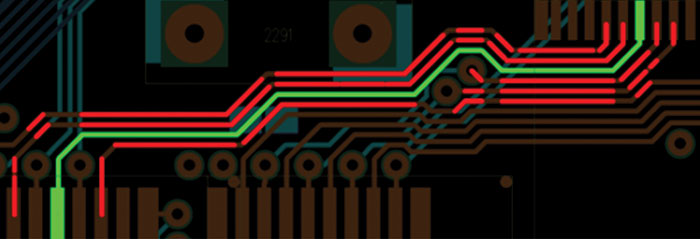
Figure 3. Proper placement of ground planes to transmission lines can inhibit crosstalk.
Rebecca Lord is technical marketing engineer at Mentor (mentor.com). She has a bachelor’s in computer engineering and was previously a hardware engineer in the data storage industry.


