
When using flex, don’t design too close to the edge.
Because flexible circuits are very thin, they are considerably more delicate than a rigid PCB, and more susceptible to damage in manufacturing and handling in the field. Damage in manufacturing is reflected in the yield rate, which directly affects board cost. Here we look at optimizing the flex circuit for yield, cost and reliability during the design stage, and validating with a flex-specific design-for-manufacturing software tool.
Padstack considerations. Most adhesives used in the manufacture of flex-circuit base materials are unfilled. As a result, adhesive-based flex can experience unchecked thermal expansion in the z-axis, which makes vias and other features prone to delamination, cracking and intermittent behavior after soldering components to the surface of the flex. The designer needs to include a more robust padstack for components placed on the flex circuit compared to the rigid area of the circuit. Pad examples are shown in FIGURE 1.
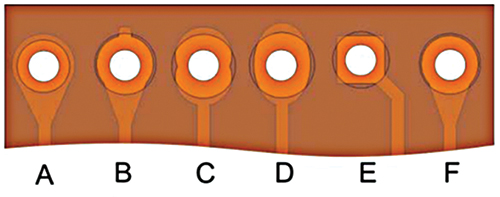
Figure 1. Various pad designs to help facilitate their capture by the cover layer: (A) Standard filleted pad with full pad capture; (B) standard filleted pad with hold-down tab; (C) overlapping pad design; (D) oval pad design; (E) corner entry to square pad; (F) plated through-holes normally require only filleting.
SMT requirements. Surface mount components can be placed on flex if supported by selectively bonded stiffeners where required. Because copper on a flexible substrate is susceptible to delamination with much less effort than a typical FR-4 board, surface mount pads require support. The most common form of support is a coverlay overlap on pads and vias. Another common method of support is enlarged pads. This gives more area for the pad to adhere to the laminate material. When both support methods are used together, robust adhesion is possible.
Coverlays. Designs using a coverlay that does not extend throughout the entire rigid portion create an area called the interface region. The interface region is the area where the flex and rigid portions of the design meet. It typically extends approximately 1.25mm from the edge of the board into the rigid area and flex area, for a combined 2.5mm region. This region tends to be more delicate than the rest of the circuit and requires special consideration. Good precautions include avoiding vias, mounting holes, slots, and plated through-holes proximate to the edge where flex and rigid join (i.e., less than 2.5mm), and use of any angle other than 90˚ where traces enter rigid sections of the circuit (FIGURE 2).

Figure 2. The coverlay is too close to a pad.
Whenever possible, pads larger than the access holes in the coverlay should be used to increase bond strength and decrease delamination events. This is equivalent to solder mask-defined pads for conventional FR-4 PCBs. However, in the case of flex designs, the coverlay adds an additional measure of anchoring to the copper features.
Improving yield. Flex-circuit designs are improved by using copper traces that flow into the flexible circuit bend. This means they travel straight through the bend without abrupt direction changes. If a direction change is necessary in the bend, the use of curves rather than sharp-angled routes will reduce the likelihood of trace cracking.
Plane hatching is important when mitigating stresses in flex bends. While a honeycomb shape (hexagon) will alleviate the most angular stresses, any hatching will have a strain reduction compared with that of a solid shape.
Tolerances for flexible circuits need to be relaxed compared to typical PCBs. Because of the materials and construction methods used, flex circuits experience shrinking, expansion, stretch, and compression differently from a rigid PCB. Greater variability in the design is necessary to accommodate these events.
A major location for failure in a flex circuit is the junction between the board trace and the pad at the end (FIGURE 3). The reason for this type of failure is the pad is often much larger than the trace leading into the pad. When flexed, because the pad does not bend as readily as the trace, a fracture is created at the joint between trace and pad.
Figure 3. Interface region issues: trace width changes, via proximity and trace angle changes.
Pad fillets improve etched yield and material strength. Fillets are appropriate when the pad diameter is greater than the connecting trace width. Acute angles at the interface between traces and pads should be avoided by using fillets to minimize the concentration of stress at the interface.
Rigid-flex requirements. With rigid-flex, a minimum of 5mm from the rigid structure to flex-circuit bend is a good rule of thumb. The chance for catastrophic failure at the interface between rigid and flex increases when the bend begins closer to the rigid section. Peeling of the coverlay from under the rigid area and exposed copper are typical failures seen when this spacing is not roughly followed.
Manufacturing flex vs. standard PCBs. Building a flex circuit generally involves the same steps from circuit to circuit. However, certain circuit designs/features can affect the ability to manufacture a cost-effective and reliable product. Conductor width is especially important in flex. A safe conductor-width rule is to use conductors at least five times as wide as they are thick. The best practice is to use the thinnest copper that will safely carry the intended signal or current and to adjust trace width accordingly.
Once the design is complete, it must be created and validated, and the manufacturing instructions communicated to both the fabricator and assembly supplier.
Often, the output for manufacturing is simply referred to as “Gerber” files, but this is a misnomer. What is actually sent is a combination of data files and drawings with notes, most generated from different sources and frequently containing conflicting information. Presenting this information clearly and understandably greatly enhances the chance of getting the product produced correctly on the first pass. However, approximately 80% of the flex documentation packages received by manufacturers require some sort of clarification.
Instead of sending multiple files of various formats and a series of drawings and documents, all the information manufacturing needs can be communicated with a single data container. This ensures efficient operation and significantly reduces potential for errors, misunderstandings, and callbacks. This container should include all the relevant information contained in data fields to be used by the receiving CAM system.
Gregory Beers is a senior application engineer for Mentor Graphics (mentor.com). He has a bachelor’s in electrical engineering and was president and principal engineer of a PCB service bureau where he specialized in rigid-flex circuit design; This email address is being protected from spambots. You need JavaScript enabled to view it..


