Arraying boards reduces panel cost and speeds assembly.
What do you think of when you hear the word “array”? Perhaps an antenna array, or possibly some type of mathematical array, or maybe even video graphics array (VGA, such as the adapter connection from a PC to a monitor)? It is one of those words that can mean something different to almost anyone who hears it.
Questions about arrays are very common in PCB manufacturing. An array combines a single PCB multiple times to make a larger group of connected boards. This process is sometimes referred to as “stepping out” the individual boards, or “step and repeat.” Other terms used to describe an array are panelized, stepped out, palletized and route and retain.
An array helps an assembler with the build process. Parts can be loaded at a much faster rate because the manufacturer can assemble the entire array at one time, instead of loading one board at a time. Boards are loaded using automated pick-and-place machines, which pick up parts (normally surface mount devices) and place them on the board.
Paradoxically, arraying boards will typically raise the cost of individual boards. This happens because fewer panels are used when boards are in an array versus when they are processed as individual boards. Although the individual board cost will rise, however, the cost of board assembly is less because of the array configuration.
General Guidelines
Each electronics assembler and manufacturer will have their own specific guidelines of how they would like to have their arrays set up for manufacturing. These guidelines provide some ideas of general practices that are fairly typical for most.
Array size. Typical sizes are 8 x 10" or 10 x 12" as the overall largest size of the array. If the PCB manufacturer is using a production panel size of 18 x 24" with a usable space of 16 x 22", then the best fit of the largest array will be 7.8 x 10.8". That will permit at least four arrays “up” on the panel. If the array size is larger than that, only two arrays will fit, and the cost per board will go up significantly. Smaller array sizes can be used for smaller individual boards and still have a good yield for each panel.
Rails. Rails are extra PCB material added to the sides of the array to permit easier handling during assembly. Rails could be on two sides or all four sides of the array. Restricting rails to two sides usually permits a few more pieces on the panel, which helps the per board cost.
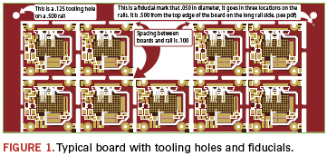
Fiducials. Typically three fiducials are needed on an array, and they usually go on the rails. The ideal size is 50 mils. The fiducial is a circle that is a copper pad with the same finish as the rest of the board on it. This provides alignment targets for the automated assembly equipment to get things lined up. Some manufacturers may require fiducials on each individual board as well. However, for the most part there are pads or other features on the individual boards that can be used to provide additional alignment targets.
Tooling holes. Tooling holes in the four corners of the array in the rails is fairly common as well (Figure 1). Again, these are used to aid alignment and orientation when assembling the board. The typical size is 125 mils, and they are non-plated.
Array spacing. Spacing depends on whether the array is scored or routed. For tab route, the spacing is 100 mils in most cases. With scoring, the boards can be placed next to one another with no spacing. Those also are the two options for “depaneling” (separating) boards after assembly.
Scoring. Scoring is the act of making a small “V” groove along the length of the board where separation takes place (Figure 2). The groove is typically one-third on top and one-third on bottom, leaving one-third of the material in place to hold the boards together.

When scoring, there should not be any parts placed within 250 mils of the edge of the board. If they are closer than that, there is the possibility that the parts could come loose during the depaneling process. If the board thickness is more than 62 mils, and the score line is a long score line, it can require a significant amount of force to separate the boards.
Tab Route. Tab route arrays will leave a small tab on all four sides of the board attached to the other boards or the rails. This type of array is not as stiff as the scored array but can be easier to break apart.
Tabs are typically one on each side of every board and usually 50 mils wide. They usually have small holes drilled on the edge of the tab at the board outline. Those small holes are referred to as mouse bites or perforated holes, or sometimes rat bites. Either way, they make it easier to break tabs off the board. They do leave a rough edge, so additional sanding or grinding might be needed for smoothness.
X-outs. An X-out is when one of the individual boards on the array does not pass test and is marked out usually with a marker. Some manufacturers will permit a certain percentage of X-outs (such as 10%) on the order, while others may require no X-outs on any of the arrays. No X-outs will make the board a little expensive, since the PCB manufacturer may need to make a larger number of arrays in order to meet the order requirements, depending on their yields.

Calculating Array Size
Many manufacturers use automated programs for calculating arrays. Here are the steps to getting a best fit array using one such program, called KwickFit.
Set panel size at 18 x 24" with 1" margins (or whatever the panel options are for whichever firm is manufacturing the PCBs) (Figure 4).

Select define array. In the Array Definition area, enter the individual board dimensions (Figure 5).

- Max. size of 7.8 x 10.8"
- Min. qty. of 1, max. qty. of 100
- Click calculate.
Using these settings, the tool will output the most number of possible boards up on the full panel and on the individual array. This works well for the majority of board sizes, up to about 4 x 4". Above that size means creativity is in order to come up with the array. Assume the largest x dimension will be 7.8 and the largest y dimension will be 10.8. Use the smallest dimension of the individual boards as the x dimension. (This also can be performed manually. A spreadsheet or a calculator makes this easier, of course.)
Step 1. Determine rail size. If the rail size is 0.5, double that (rails on both sides) and then deduct that from the total available dimension for the x dimension. That would then be 1" deducted from 7.8" = 6.8". That is the “usable” space for the array in the x dimension.
Step 2. Add your spacing to the size of the board. For example, the board is 1" and the spacing is 0.1". Added, that’s 1.1".
Step 3. Determine how many will fit. Divide 6.8 by the individual board size with the spacing added. In this case, 6.8 divided by 1.1 = 6.1. So six boards of 1" size fit in the x dimension using 0.1 spacing with 0.5 rails.
Step 4. Add together. Note: Because there are spaces on both sides of the boards, add 0.1 to the total of the boards to get the correct overall dimension.
The total for the x dimension is 6 pcs. * 1.1 = 6.6 + 0.1 (for the extra space) = 6.7 + 1 (for rails) = 7.7" in the x dimension
Perform the same process for the y dimension.
10.8 – 1 = 9.8" usable space
9.8 / 1.1 = 8.9 (rounded down), or 8 wide in the y dimension
8 * 1.1 = 8.8 + 0.1 = 8.9 + 1 (for rails) = 9.9" in the y dimension.
The result is 6 x 8 up (48 pieces) and the overall size will be 7.7 x 9.9 with 500 mil rails and 100 mil spacing.
This can be calculated manually as shown here, or by using an array calculator (such as at bayareacircuits.com/pcb-array-calculator/), which makes the calculations and provides a graphical image (Figure 6).

Peter Brissette is head of PCB sales and marketing at Bay Area Circuits; This email address is being protected from spambots. You need JavaScript enabled to view it..