With the right tool, embedded passives are as easy to design into a PCB as traditional externally mounted components.
One of the largest categories in electrical components is discreet passive components: resistors, capacitors and inductors; These existed long before active devices. They have been mounted on the outside of printed circuits boards (PCBs), either with through-hole leads or with terminations all on a single side (surface mount), with the interconnection traces embedded inside or outside of the board. Increasing component density created competition for this valuable surface real estate, and new technology to embed electrical components inside the board was developed. Assembly techniques have expanded to the placement of very small, discreet SMT passive components inside the board, permitting the normal multilayer board pressing operation to encapsulate these placed components. This technology has now expanded to include active devices, like transistors and integrated circuits. Embedded passives offer many advantages over discrete components. The performance requirements, the range of resistor and capacitor values and the product size targets however, dictate when it is best to implement these passives in embedded or discrete forms.
The advantages include: lower component costs, lower assembly / ICT costs, reduction in electrical parasitic, fewer solder joints to fail and a smaller final board size. The disadvantages include: higher PCB materials costs, higher PCB process and test costs, limited range of components that can be replaced, limited reworking and modification during engineering, cost of prototyping, increased complexity in design and BOM realization.
The embedded passive materials come as bulk sheet resistances, additive screen printed pastes, additive plated thin-films or deposited dielectrics for capacitors. These materials can also be roller-coated or inkjet printed onto the inner layers of a PCB.
Resistors, discrete or formed, are actually very poor conductors when compared to copper because their function is to restrict the flow of electricity in a circuit. The common composition of resistors includes metal oxides, carbon particles or small conductive particles separated widely by an organic polymer.
For embedded resistors, the materials are classified by their ohms per square (Ω / ¨).
Capacitors can be conventional discrete or, a whole capacitance sheet may be used as distributed capacitance. Distributed capacitance is the storage of energy between the power and ground layers by employing a dielectric. In addition to offering a method of storing energy for fast-switching components, this also couples power to ground and provides lower power supply impedance. Noise on the power bus can be attenuated in this way.
Designing with embedded passives (EP) adds significant complexity, as well as risk of failure. In the traditional design methodology, all phases of embedded passive design were made by hand and sometimes assisted by custom scripts. Using the right EDA design tools can help manage the complexity and mitigate the risks. For brevity, this discussion is limited to resistors, but the principles are similar for embedded capacitors.
In some EDA tools, all this is done automatically in an embedded passive planner. The design doesn’t have to be 100% complete – the minimum requirements are to define all the resistors and/or capacitors and their properties such as nominal value, tolerance and power rating.
We can, for example, filter out all resistors with a tolerance we can’t achieve (in case we want to avoid trimming). We can also, for each available material, calculate the hypothetical dimensions of each component value and compare these dimensions to what we think is reasonable. For rectangular resistors, typical acceptable aspect ratios are between 0.2 and 15.
Whether the component falls within the acceptable aspect ratio or not, we can flag it as good or bad for each material. We can also calculate the actual component’s size so we can sum up the total component area. With these parameters, we can easily see which components can be embedded, which material(s) give the best result and the total board area occupied by the embedded parts.
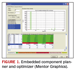
I’ll close with a brief example of how embedded passives can be incorporated into a design with available EDA tools. The screen capture in
FIGURE 1 shows a typical analysis scenario. This example design uses the Ohmega Ply 100 ohm/sq material, allowing you to embed 445 resistors, leaving just five as surface mount devices. You can also see that if you had picked the 25 ohm per sq. material, you could have embedded the last four resistors, but at the cost of more than twice the component area. The outcome of the analysis is a selection of resistors and/or capacitors to embed and a selection of the material or materials to be used.

With the embeddable component selected and the right material(s) chosen, the synthesis tool can automatically generate the components. This was traditionally a manual, and seriously error-prone, process. The synthesis can generate resistors and capacitors in different forms (in order, top to bottom in Figure 1). Now, embedded passives are as easy to design into a PCB as traditional, externally mounted components.
PCD&FHappy Holden is a senior technologist at Mentor Graphics. He can be reached at
This email address is being protected from spambots. You need JavaScript enabled to view it. and http://blogs.mentor.com/happyholden/.


