Controlling via impedance and minimizing reflection are important when designing via structures because via-hole transitions are a major contributor to signal degradation.
The design of controlled impedance via holes with minimal reflection is an especially important task for interconnects that have data rates of 6 Gb/s and higher, with the signal spectrum in the microwave frequency band. Via holes are structures connecting components and traces in different layers of a multilayer PCB or package. They are relatively small when compared to the traces and behave almost like ideal connections at low frequencies, due to their small electrical length and small impedance of the current return path. Because of that, the via holes are often either completely ignored during analysis or simulated with a lumped inductance and/or with a lumped capacitance, calculated with approximate equations. This was working fine until recently, when the spectrum of signals transmitted through the interconnects reached the microwave range (above 3 GHz for 6 Gb/s signals). The via holes behave as distributed structures at these frequencies and must be simulated as the distributed structures.
Unfortunately, not all vias are identical from the analysis point of view, and some classification of different vias may be helpful before even approaching the analysis. Some via holes can be simulated in isolation from the rest of the board, while others may require the analysis of the whole board, with all reference and power distribution structures included. The vias from the first group can be termed as localizable, and I will explain how to distinguish and to design them.
Current Return Path
Via holes are often classified by the span in a board stack-up as through, buried, blind, back-drilled, etc. Via-hole current return path localization may be used to separate the vias into two groups for analysis purpose. Via holes with the current return path in a small area around the via can be called localizable. Otherwise, if the current return path is spread over the board, the via can be called non-localizable. Via holes that connect traces with the same reference planes always can be analyzed in isolation (though they may radiate). This is not the case for vias connecting traces with different reference planes (via holes crossing one or more reference planes). Let’s investigate the return current localization separately for single-ended and differential via holes, with three different cases shown in
FIGURE 1. They can be defined as follows:

1. Planes that are not connected or terminated, and the return current is the displacement current between the planes. The problem is non-localizable for broadband analysis (
FIGURE 1a) and requires analysis of the entire board.
2. Planes that are terminated with the decoupling capacitors, and the return current is a combination of the displacement currents through capacitors and planes (
FIGURE 1b). Capacitors have low impedance only in a narrow frequency band; thus, the problem again is non-localizable for broadband EM analysis.
3. Stitching vias that are used to connect the reference planes for the connected layers, and the return current is mostly conductive (
FIGURE 1c). The problem can be localized (localizable) and solved with any boundary conditions, though the frequency band may be limited.
For multi-gigabit signals, single-ended vias always require electrically close stitching via holes that join all reference conductors of the connected transmission line. Stitching via holes at a quarter wavelength distance (3.75 mm or 147 mil for 10 GHz for instance) do not provide the path for the return current, and the structure becomes non-localizable. This is similar to a short-circuit condition in a t-line that becomes an open circuit if the t-line segment length is equal to one-quarter of the wavelength. For practically, the localizability property of a via hole can be estimated by investigation of S-Parameters dependency, either on the boundary conditions and simulation area in an electromagnetic simulator or on the geometry and size of a board in experiment.
Localizable via holes are relatively independent of the simulation area or board shape and size. They can be simulated in isolation from the rest of the board and reliably reused as a design component. Note that all reference planes of the connected transmission lines have to be connected by the stitching vias – otherwise, the structure is not localizable by design. Not-localizable cases are usually difficult to simulate with a 3D full-wave analysis, and parallel-plane (transmission plane) models may be used at lower frequencies, while hybrid models may be required at higher frequencies. Anywhere from four or more stitching via holes per signal via may be required to maintain localization up to 20 GHz on a typical PCB.
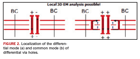
Differential vias are a two-via transition through multiple parallel planes, with possible stitching vias nearby. Two excitation modes can be defined for a symmetrical pair: differential and common (similar to differential t-lines). The differential mode has identical currents in both barrels, flowing in the opposite direction, and the common mode has two identical currents in the same direction. Differential pair signals always contain differential mode (useful) and may contain common mode induced by asymmetries in the driver and by discontinuities.
If two barrels are electrically close to each other, the differential mode is localizable and can be simulated with any boundary conditions at a sufficient distance, as shown in
FIGURE 2a. The common mode behavior is similar to the single-ended via and is not localizable without stitching vias nearby. Electrically close stitching vias may be used to confine the common mode and to simulate the structure in isolation from the rest of the board, as shown in
FIGURE 2b.

If stitching vias are not used to localize the common mode, simulation of the whole board in a 3D full-wave solver with all plane terminations may be required. As in the case of single-ended vias, it is rarely possible and not practical. Use of a hybrid solver with 2D transmission plane models is practical, but accurate only if such solvers include 3D full-wave models for differential mode. On the other hand, accurate analysis of the might not be differential vias with common mode may be not required if common mode is relatively small by design.
1S-Parameters
Scattering parameters is a natural black box description of a linear system in the frequency domain. The system can be smaller, comparable with or larger than the wavelength. All types of via holes and the complete interconnect parts of a data channel can be accurately characterized with S-Parameters. For serial channel analysis, via hole S-Parameters and other components are usually concatenated and simulated either in frequency or in time domain with driver and receiver models. S-Parameters can be computed with an electromagnetic simulator or measured with a Vector Network Analyzers (VNA) or by post-processing TDR/TDT responses (less accurate but may be acceptable for analysis of serial channels). Thus, S-Parameters are the best choices for precise validation of interconnect models. S-Parameters of an N-port structure is N by N matrix (2 by 2 for 2-port single ended channel).
Each element of the S-matrix is

a ratio of a wave
b1 either reflected from or transmitted through the structure to the incident wave
aj. The waves are defined as a simple but very important transformations through voltage and current at a port i:

where Z
0 is the normalization impedance (usually 50 Ohm).
All elements of an S-matrix are complex numbers with a magnitude ranging from 0 to 1 for passive structures. Diagonal elements of an S-matrix characterize the reflection from the structure. All elements of a channel, including vias, must be designed to have minimal reflection over the frequency band of interest (minimum of differential mode reflection for differential via-holes). Off-diagonal elements are either useful transmission coefficients or non-desirable coupling or transformation coefficients. Ideal loss-less interconnect has a transmission coefficient of 1. All elements of an S-matrix are unitless, but they can be expressed in dB as

Minus infinity dB corresponds to an ideal non-reflective structure. Everything above it is the reflection loss, and 0 dB corresponds to the ideal transmission through the structure. Everything below it is the transmission loss.
Modeling Via Holes
There are no simple via-hole models in microwave frequency range for analysis of multi-gigabit signal propagation (especially if vias are going through multiple parallel planes). Electromagnetic analysis is usually required. We can distinguish three different approaches: distributed LC models, transmission plane models and 3D full-wave models.
Distributed LC models, with ladder-type connections of capacitances and inductances,
2,5 are similar to a lumped LC model of a transmission line. They work well for localized via holes at a lower data rate or slow edges (signal spectrum up to 1 GHz to 3 GHz). L and C values can be calculated with a static and magneto-static solver or with the infinite radial waveguide or parallel-plane models.
Transmission plane models are good for non-localizable cases for signals with spectrum up to 3 GHz (may be extended by hybridization with 3D models). Impedance of power distribution parallel planes is computed to simulate a current return path.
3-6 Parallel-plane structures have low impedance by design at these frequencies, and even simplified models are sufficient to predict behavior of vias. Both distributed LC and transmission plane models usually ignore the non-circular shapes of anti-pads (oblong or rectangular) and do not account for the transition from the trace to via holes. That is why they may be considered as the first approximation for a serial channel analysis.
3D full-wave electromagnetic analysis is a solution of Maxwell’s equations in 3D space with all field components and displacement term included. Transition from transmission lines to vias and geometry of pads and anti-pads are usually included in such analysis. Signal and return path currents have to be confined into a small area electrically isolated from the rest of the board. Geometry of the via-hole barrel, pads and anti-pads can be adjusted to minimize the signal reflection over the frequency band of interest. There are many electromagnetic solvers on the market that can handle such localizable cases. Analysis of non-localized structures with a 3D full-wave solver may require geometry of the whole board and is usually not practical because of extremely long simulation times and no possibility to reuse the same via at different locations on the board.
Designing Localized Vias
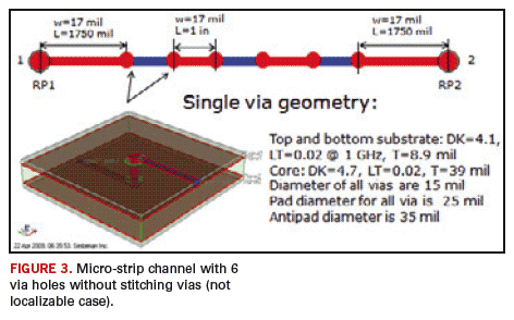
Three structures are used as examples. The first structure is a micro-strip channel with 6 single-ended via holes without stitching vias, as shown in
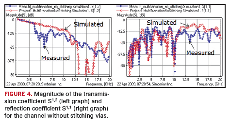
FIGURE 3. The via holes are not localized (change of reference planes and no stitching vias nearby) and thus, cannot be simulated in isolation from the rest of the board. But if we do such analysis, we can observe good correspondence of the transmission and reflection at frequencies up to 3 GHz, as shown in
FIGURE 4. This is because of the low impedance for the current return path provided by the parallel planes and by some remote stitching vias at low frequencies. Resonant properties of the board show up at higher frequencies, and the whole board has to be simulated to predict behavior of the vias.


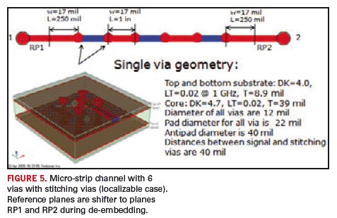
The second structure is the same micro-strip channel, but each signal via hole is isolated with four stitching vias, as shown in
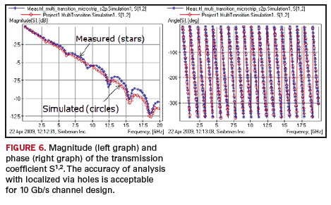
FIGURE 5. The stitching vias minimize the impedance of the return path up to 20 GHz and allow local electromagnetic analysis. The via-hole geometry has been optimized to have minimal reflection, and the reflection from the actual via hole on the board was larger than predicted, probably due to either manufacturing tolerances or weave effect. The final via geometry is relatively close to optimal and acceptable for practical 6 Gb/s to 10 Gb/s data channels. The magnitude and phase of the transmission coefficient is shown in
FIGURE 6.


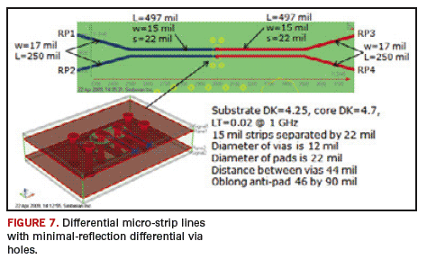
The final structure is a differential transmission line with differential via holes, shown in
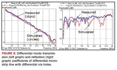
FIGURE 7. As in the case of the single-ended via hole with stitching vias, the geometry of the differential vias has been synthesized with Simbeor 2008 software to minimize the reflection of the differential mode. Four stitching via holes are used around the differential via holes to localize the common mode. The final via holes are acceptable for 6 Gb/s to 10 Gb/s transmission, and the model shows good agreement with the measured data, as shown in
FIGURE 8.


Correspondence in the common mode transmission and reflection was also acceptable due to use of the stitching vias.
Conclusion
It was shown that all via holes can be classified as localizable and non-localizable. Only localizable via holes can be reliably simulated with a 3D full-wave solver in isolation from the rest of the board and safely used in multi-gigabit serial data channels. On the other hand, non-localizable via holes may require board-level analysis with all power distribution structures included. Reliable analysis of non-localizable vias at microwave frequencies is practically an impossible task and such vias should be avoided by design. Single-ended via holes can be localized with electrically close stitching vias, connecting all reference planes of the connected transmission lines. Differential via holes are localizable for differential mode only if the barrels are electrically close. Common mode of differential via holes can be localized with the stitching vias, similar to the single-ended vias. In addition to the localization, the via-hole geometry has to be optimized to have minimal reflection loss over all frequency bands of interest to minimize the effect of resonances created by reflections between via holes. It was demonstrated that localizable minimal-reflection single-ended and differential via-holes can be successfully designed for 6 Gb/s to 10 Gb/s channels with good correspondence of simulations with measurements.
PCD&FREFERENCES
- “Practical notes on mixed-mode transformations in differential interconnects (with experimental validation),” Simberian app note #2009_01, available at http://www.simberian.com/AppNotes.php.
- E. Laermans, J. De Geest, D. De Zutter, F. Olyslaget, S. Sercu, D. Morlion, “Modeling Complex Via Hole Structures,” - IEEE Trans. on Adv. Pack., vol. 25, 2002, N2, pp. 206-214.
- H. Liaw, H. Merkelo, “Simulation and Modeling of Mode Conversion at Vias in Multi-layer Interconnections,” ECTC 1995, pp.361-367.
- Y. Shlepnev, “Transmission Plane Models for Parallel-plane Power Distribution System and Signal Integrity Analysis,” - in Proc. of 22nd Annual Review of Progress in Applied Computational Electromagnetics, Miami, 2006, pp. 382-389.
- C. Schuster, Y. H. Kwark, G. Selli, P. Muthana, Developing a physical model for vias, - DesignCon 2006, available at http://www.designcon.com/infovault/
- G. Selli, C. Schister, Y.H. Kwark, M.B. Ritter, J.L. Drewniak, “Developing a Physical Model for Vias – Part II: Coupled and Ground Return Vias,” DesignCon 2009, available at http://www.designcon.com/infovault/
Yuriy Shlepnev is president of Simberian Inc. and can be reached at
This email address is being protected from spambots. You need JavaScript enabled to view it..


