Manufacturing methods, like screen-printed paste, are giving way to
photolithography, inkjet deposition and plating, as solar cell
manufacturing techniques evolve.
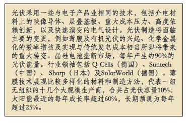
Photovoltaics (PV) is the
electronic industry’s younger brother. Each industry shares some DNA -
imaged conductors on dielectric material, layered substrates, severe
cost pressures, high dependence on innovation and rapidly evolving
electrical designs. But the sibling industries are enticingly
different. During 2007 and 2008, I embarked on a fact-finding tour into
the world of solar cells, with the charter to learn the players,
markets, issues and drivers that are shaping this rapidly growing
industry. Just like the older brother PCB industry of 1960 through
1990, PV is on a rapid growth spurt.
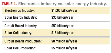
TABLE 1 gives a snapshot
of where we are today. There are major changes in store for PV’s
adolescence, such as the emergence of thin-film and organic
photovoltaics, the efficiency gains of chemical metallization and the
soon-to-come huge transition from achievement of grid-parity. Who will
win – silicon, thin-film or organic PV? Germany, China or the US? IC,
PCB or green-field PV makers? Cast away your preconceived notions; it
will require a fresh look to synthesize the wish lists from leading
solar cell makers and to uncover the real opportunities for
next-generation PV.

Efficiently utilized, my body’s mass would
provide enough energy to power the country’s electricity demand for one
month. That is, if you believe Mr. Einstein. We need to take his
calculations somewhat on faith. E=mc² predicts that my mortal coil of
95 kg is equivalent to 2.2 trillion kilowatt-hours of power. Per the US
Energy Information Agency, that would power us from June to July. We
would need trainloads of coal, pipelines of natural gas, billions of
barrels of oil and countless splittings of uranium to make up the rest.
These alternatives are, by the way, the sources of energy production in
America, in order of power supplied.
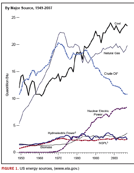
FIGURE 1 shows US energy
use. Coal is dirty, producing dust when mined, sulfur when burned and
acid rain when washed from the sky. Natural gas is expensive to find,
more expensive to transport and produces greenhouse gases when
combusted. Crude oil combines the ills of coal and natural gas and adds
other problems. Oil is dirty, expensive, in limited supply and
necessitates reliance on a supply chain outside US boarders. Nuclear
energy is on the rise, now contributing about 7% of domestic power but
suffers from “not in my back yard” concerns over new plant locations,
safety and spent fuel disposal. Rounding out the list of energy sources
are biomass, wind, hydroelectric and solar power. I should clarify that
just about all of the energy sources listed above are really just
different manifestations of solar energy. Fossil fuels are made from
the anaerobic metamorphosis of plants, which stored solar energy as
carbohydrates long ago – same story with biomass, just on a more recent
timescale. Wind results from sun driven weather patterns. Only
hydrothermal and nuclear fission, deriving their power from the
radioactive decay of earth itself, are independent of the sun.

Catching Photons
The
sun emits 370 billion petawatts. Metric prefixes haven’t reached this
level of quantity yet, so the best I can do is say 370 yottawatts – no
kidding. Luckily for us, energy diminishes with the square of distance,
and our atmosphere screens the level down to about 1000 watts per meter
at Earth’s surface. That is a lot of power, enough, if converted
efficiently, to power two 70-inch plasma TVs. That’s the trick –
converting this boundless source of energy in an efficient way. For
more than 100 years, scientists have been trying to convert photons to
electrons efficiently. The 1950 vintage solar cell converted solar
energy to electricity at about 5% efficiency, while today’s production
model is more like 15%. Why so low? There are a few factors limiting
the amount of electrons produced per sunlit area. Most solar cells are
made from crystalline silicon, doped with boron and phosphorous to
produce a p-type/n-type junction. The theoretical maximum efficiency of
such a system is about 25%, but to get captured, the photons need to
reach the p-n junction. The photons might bounce off the cell’s
surface, reflect back into space or pass right through the cell if
their wavelength is wrong. Some of their energy will be wasted if they
are too strong or never captured if they don’t exceed the band-gap
energy. When the photons do get captured, again proving Einstein’s
Nobel-winning photoelectric effect, they will generate an exciton – a
separated charge. The electron and hole pair will need to reach their
respective destinations to complete the electric circuit without a
fatal recombination, or all that energy will be for naught. Successful
electrons will suffer resistive losses in the silicon, at the interface
with the conductors and within the conductors themselves. Cumulatively,
these effects and others bring production cells to about 15%
efficiency. This is where innovation promises to save the day; newer
designs reduce shadowing, improve conductivity, minimize reflection and
place the junctions closer to the conductors. Lab cells with
efficiencies above 24% are translating into production cells with
efficiencies above 20% at the high end.
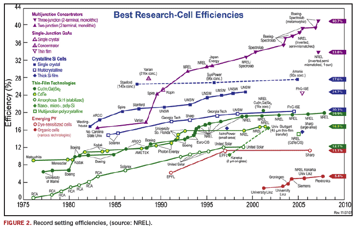
FIGURE 2 shows some of the record-setting efficiencies.

Solar Power Players
Crystalline
silicon cells dominate the market, accounting for about 90% of the PV
energy produced annually. Industry leaders Q-Cells (Germany), Suntech
(China), Sharp (Japan) and SolarWorld (Germany) make most of their
cells using silicon wafers with a silver conductive front-side grid
made from sintered screen-printed silver paste and aluminum and silver
paste back side. SunPower, a US company, takes silicon in a new
direction by forming all conductors on the rear side, freeing up the
front for full light absorption. Japan’s Sanyo incorporates layers of
photosensitive silicon – crystalline and amorphous – in its HIT design.
While First Solar's (US) take is unique among PV leaders with use of
non-silicon thin-film technology, utilizing cadmium and telluride.
Other silicon innovations include novel wafer growing methods at
Evergreen (US) and Schott (Germany) and unique conductor formation with
Suntech’s Pluto cells – a new take on BP Solar’s mothballed laser
trench process called Saturn.
Thin-film technologies, as is
common with newer industry sectors, exhibit a much more diverse set of
materials and manufacturing methods, representing a fragmented set of a
dozen or so sizable producers totaling about 10% of PV capacity. Like
the PCB industry, PV loosely follows the 80/20 rule, with the top 20
solar cell producers generating close to 80% of the industry’s total
revenue. Similar to the PCB industry, the usual cast of characters
represent the solar energy manufacturing regions – Japan, China,
Germany, Taiwan and the US. Similar, too, is the trend toward
technology transfer from western R&D labs to production
manufacturing in Asia. This trend will not be as dramatic in PV,
however, because the large, heavy, fragile PV modules are best built
near the location of their intended use. The consumption of solar cells
relies on different drivers than our electronics experience.
Consumption is based on government subsidy. This explains the quick
change from Japan’s consumption of 36% of the world’s PV power in 2002
to just 9% in 2007, while Europe now purchases about three-quarters of
PV power, thanks to attractive government incentives in Germany and
Spain. Late in 2008, Congress extended the Investment Tax Credit. Will
the US be the world’s next leading consumer, thereby benefiting from
the inevitable rise in domestic manufacturing? The stimulus package
might be the deciding vote.
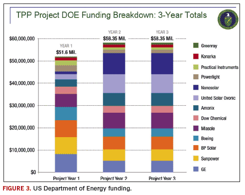
America is no slouch in funding
alternative energy, even before “Obama bucks” come rolling in. The
Department of Energy’s Solar America Initiative funds companies and
universities in its Technology Pathway Partnership to the tune of about
$60 million per year. The DOE programs, as well as the state- and
federal-level tax benefits, will grow dramatically once the $787
billion American Recovery and Reinvestment Act (stimulus) funds begin
allocation, with $45 billion slated for the Energy and Green Jobs
Program. These funds, mirrored in spirit in Japan and Europe, are
enough to stoke the jealousy of the under-represented electronics
industry around the world. Those interested in tracking the US funding
can do so at: www1.eere.energy.gov/solar and www.recovery.gov. Overall,
the plan is to bring the cost of solar-generated power equal to, or
below, the cost of conventional power – the magic threshold known as
grid-parity. With this achievement, the manufacture of PV will explode
in growth.
FIGURE 3 provides an overview of DOE TPP funding.
Guessing on Growth
Everyone
understands the appeal of solar power; it’s clean, quiet and a
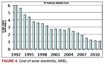
renewable energy source. However, it has also been billed as expensive.
As solar power efficiency makes its unrelenting climb upward, the
cost/watt continues its descent.
FIGURE 4 maps the cost of
solar electricity. You can argue that the efficiency increases will
slow, following the law of diminishing returns, as we approach the
theoretical max of solar energy conversion, but the cost declines will
accelerate, as the industry matures. More companies will join,
manufacturing efficiencies will improve, material costs will drop and
equipment will be amortized, but this industry’s growth is not governed
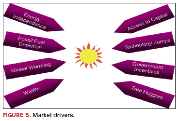
solely by the laws of Economics 101. Other factors, like we saw with
government incentives, are at play.
FIGURE 5 lists the market
drivers. Forward thinking environmentalists and technogeeks were the
early adopters of solar power. Not concerned with ROI, these groups buy
PV regardless of the price. Others, with no access to grid electricity,
will also pay any price. We see the use of solar modules in remote
Africa, in the Rocky Mountains and even in outer space. Don’t dismiss
those who wish to control their own power source, from the survivalists
in New Mexico to the suburbanite in New Jersey with back-up PV. But
when we move into the political realm, all bets are off. Global warming
and pollution are touchstone issues galvanizing the lobby to expand
solar energy. With a government anxious to reduce dependence on Middle
East oil, we can begin to understand the success of solar subsidies in
the US. Feed-in tariffs in Germany, Spain, Italy and Greece pay solar
households €0.30-0.55/kWh, (currently about $0.41 - $0.75/kWh) and have
shown such popularity that we can expect an expansion of pro-solar
policy worldwide. Solar power has achieved its tipping point. Recent
annual growth rates exceeded 60%, with long-term forecasts at more than
25% per year. Efficiency increases, material cost decreases, production
and consumption incentives, as well as economies of scale, are all
conspiring to catapult PV into big-time deployment. The current credit
crisis is indeed slowing the flood, but only temporarily, as some
investors see the investment return from PV generation as more
attractive than alternative, low-risk investments. With apologies to
Lao Tze, the journey to grid parity begins with a thousand small steps.
Bigger steps will come through design and manufacturing innovation. To
understand the opportunities for innovation, look at the weaknesses of
existing solar cell technology.


The Power Maker
Conventional
“first-generation” solar cells are made using crystalline silicon
wafers, often of a lower grade than silicon used in semiconductors. The
Si (+4) wafer starts as p-type with boron (+3) dopant. To better
capture light, the wafer is textured with hydroxide or
nitric/hydrofluoric acids to generate mountainous geometry intended to
reflect light obliquely into the silicon. The p-n junction is formed
with diffusion of phosphorous using vapor deposition, and a surface
passivation is applied, again in vacuum equipment, to impart the
characteristic blue silicon nitride film. Among these steps, wet
chemical processes are interspersed to clean, to neutralize and to
prepare the silicon along the way.
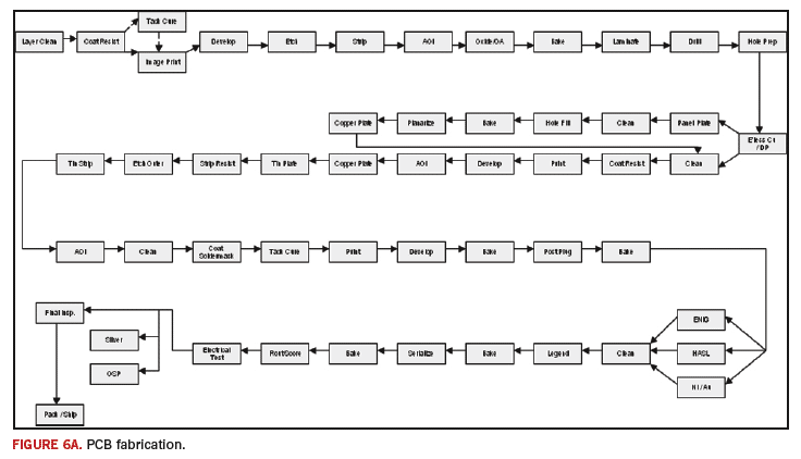
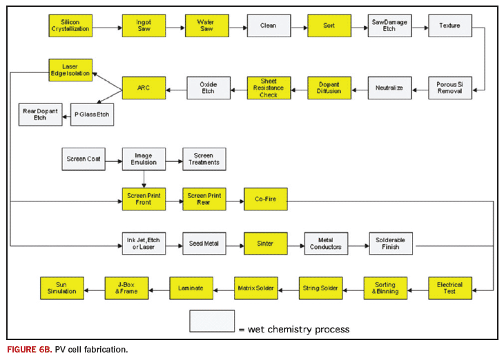
FIGURE 6a and
FIGURE 6b compare PCB and PV manufacturing processes.


Our
silicon wafer is now an energy-producing diode, but without the means
for extracting those electrons for useful work. The ensuing conductor
formation step, creating elemental circuitry on the cell’s surface,
begins to remind us of the early days of the PCB industry. A conductive
silver paste is screen printed on the sunny side of the wafer. The
paste is sintered at 900ºC, an obscenely high temperature necessitated
not just by the sintering of silver flakes, but in an effort to break
through the silicon nitride with tiny glass frits contained in the
specialty silver paste. Meanwhile, the circuit is completed on the dark
side of the cell with aluminum and silver paste – silver to make
contact with silicon and aluminum to form a back surface field. The +3
valence of aluminum helps boost the p-type nature of the junction. For
circuit builders, screen-printing is so 1960s, but screening rules the
PV world. Rebellions are springing up in various quarters, however.
Sunpower and Suntech famously use sputtering and photolithographic
techniques, borrowed from a semiconductor lineage, to make better
contact. These companies (and others) also apply the cost advantages of
the PCB world by building the conductor with wet plating chemicals.
Patterns of Success
Conductor formation techniques, as an alternative to screen-printed paste, can take several incarnations:
- Inkjet resist and etch of anti-reflective coating (ARC)
- Aerosol deposition of silver paste
- Inkjet deposition of metal paste
- Laser ablation of ARC
- Photolithography
In
any case, the replacement of screened paste means that some other
method for building a conductor is needed. The PCB industry knows all
about these techniques: electroless and electrolytic metal plating.
Imagine a silicon wafer with a phosphorous-diffused emitter and an
aluminum-back surface field. Resist patterning of the wafer’s front,
followed by fluoride etching of the silicon nitride anti-reflective
coating, would result in exposed silicon. A very thin layer of
electroless nickel can be used to make electrical contact to the
silicon. A low temperature sintering operation bonds the conductor to
the silicon by formation of the nickel silicide intermetallic phase.
Once the nickel is locked in place, several options are available to
build a suitable conductor. Copper is cheap and nicely conductive, but
it requires a thin nickel layer to prevent copper from poisoning the
silicon; both metals are easily plated on the wafers. There is a trend
toward electroless processing, since the connection of very thin wafers
in electroplating can cause breakage of these fragile specimens. One
elegant idea has been resurrected from semiconductor’s past – the use
of the current produced by the cell itself to fuel more metal
deposition, a process termed “light-induced plating”. Whatever the
sequence and technique, deposition of metals from wet process chemicals
will bring the cost, handling and productivity benefits needed to get
solar cells to grid parity.
Non-Silicon
While much of the
solar cell industry relies on crystalline silicon wafers (~85% by
wattage produced,) there is a growing class of alternatives, looking to
evade the cost and processing disadvantages of conventional PV. The
most noteworthy segment – thin-film – is represented by a set of
techniques where thin coatings of photosensitive materials are
deposited on (usually) a rigid glass substrate. The material must meet
the requirements of converting energy from ambient light into
electron-hole pairs and allow the charge separation through the act of
semi-conductivity. Surprisingly, many materials exist to meet these
requirements.
TABLE 2 shows some of the PV manufacturing
options. The US is especially active in the thin-film sector,
possessing a very active group of R&D facilities and startup
ventures based on thin-film. What is not possible, when discussing
thin-film PV, is use of broad generalizations like we used when
describing silicon PV. There are dozens of photosensitive materials
(CdTe, CIS, CIGS, amorphous Si, etc.), several substrate platforms
(glass, steel, organic films, etc.) and even a fascinating set of
installation techniques. If this complexity weren’t enough, yet another
generation of PV methods is upon us, employing superconducting
buckyballs, dye-sensitized organics, multiple heterojunction layers for
capturing various photon energies and even nano-structured antennae for
plucking electromagnetic wavelengths directly into high-frequency
electricity (solar energy in the dark!)

What to do?
In our
age of limited resources, perhaps the only thing more abundant than the
sun’s energy is the unbridled enthusiasm over solar energy. Guilty, I
am an unabashed enthusiast! A degree of caution is due to counteract
the solar lovefest. I cannot recommend a mass exodus of professionals
and capital from the strong and mature electronics industry to the more
speculative PV industry. The learning curve is a long path, with
profound changes happening daily. I hope my comparison of the PCB
industry to PV leads to the conclusion that some processing techniques
are similar, but there are many other aspects that vastly separate the
sibling technologies. While I will warn you that the path to the sun is
long and difficult, I will also remind you of Icarus’ inspirational
quote, “All limits are self imposed.” Then again, flying too close to
the sun, Icarus found some limits externally imposed.
PCD&FDon Cullen is managing director at MacDermid Photovoltaics Solutions and can be reached at
This email address is being protected from spambots. You need JavaScript enabled to view it..


