Photovoltaics, displays and sensors could lead an industry revolution.
In 2007, the iNEMI Roadmap included (for the first time) a chapter titled Organic and Printed Electronics. For the 2009 edition, the scope of this chapter has been expanded to include the variety of technology platforms being investigated in this emerging field. Also, the name of the chapter was changed to Large-area Flexible Electronics to reflect this broader technical scope, and to be “agnostic” to materials (organic, inorganic, hybrid) and manufacturing processes (printing, vacuum, lithography).
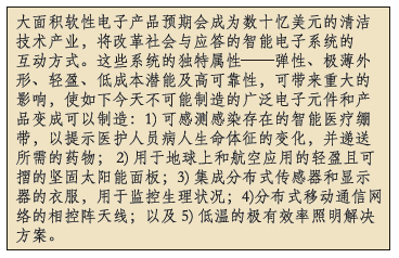
Large-area flexible electronics is expected to become a multibillion-dollar clean-tech industry that will revolutionize how society interacts with intelligent and responsive electronics-based systems. The unique properties of these systems – flexibility, ultra-thin profiles, light weight, potential for low cost and high reliability – could have enormous impacts on consumer electronics, aviation and space electronics, life sciences, lighting, power, military applications and telecommunications. They will enable a broad range of electronics components and products that are not possible today, such as: smart medical bandages that sense the presence of infection, alerting medical staff to changes in a patient’s vital signs and delivering needed medication; lightweight, foldable, rugged solar panels for terrestrial and space applications; clothing with integrated distributed sensors and displays for physiological monitoring; phased array antennaes for distributed mobile communications networks; and low-profile, ultra-efficient lighting solutions.
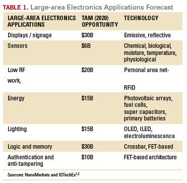
Industry analysts, as well as trade associations, have identified a broad range of possible applications and components (TABLE 1). The systems listed will be composed of organic, inorganic or hybrid materials, and fabricated via large-area mass manufacturing processes.

Several factors are leading this emerging industry, including: development of higher-performance solution-process-able semiconductor and photoactive materials (e.g., organic small molecule, inorganic precursors and inorganic nanoscale material suspensions); commercialization of large-area processing equipment; qualification of large-area flexible electronics manufacturing practices by adopting practices from the microelectronics, semiconductor and roll-to-roll processing industries such as printing; and advances in the design and layout tools necessary for product development.
The roadmap working group identified three near-term opportunities for large-area flexible electronics: displays, photovoltaics and sensors.
Displays
Displays are expected to offer the first commercialization opportunity for large-area electronics, including point-of-purchase signage, electronic books, PDAs, GPS/electronic maps, automotive displays and instrumentation panels and smart cards.
The display module consists of an electronic control element (backplane) and an optoelectronic visual element (front-plane). Several companies are currently developing large-area processes to fabricate active matrix backplanes consisting of arrays of organic semiconductor-based transistors, with hopes for commercial launch in early 2010. The first product offerings are expected to be mobile devices having large-area flexible displays.
Long term, the vision is to offer a large-area flexible color display for viewing topographic maps, streaming news, magazines, books, etc., which, when not in use, can be folded and placed into one’s pocket. To achieve this long-term vision, several technology features must be developed or enhanced to ensure continued commercial launches of new products integrating large-area flexible displays and greater product acceptance by the mass market such as:
- Improved wireless functionality. The ability to offer pseudo-streaming will provide greater product flexibility and new products.
- Availability of vivid color gamut. In the past, filters have been used to demonstrate color, but this approach reduces resolution by approximately one-third. An alternative approach is necessary.
- Increased flexibility of large-area displays. The majority of products that will be introduced later this year rely on a multilayer display module structure that reduces the display flexibility.3 The introduction of a truly rollable/foldable display will provide designers freedom in developing products with novel form factors.
- Improved refresh rate. Screens typically refresh at rates slightly faster than one frame per second. Several leaders in this field have begun to develop novel materials and driving schemes to provide video rates (24 frames to 30 frames per second) without flicker.4
Photovoltaics
Another near-term large-area electronics opportunity is fabrication of photovoltaic modules. Several companies have well-staffed activities to develop processes (e.g., printing, roll coating) for the deposition of photoactive materials in an effort to establish a reel-to-reel manufacturing platform.
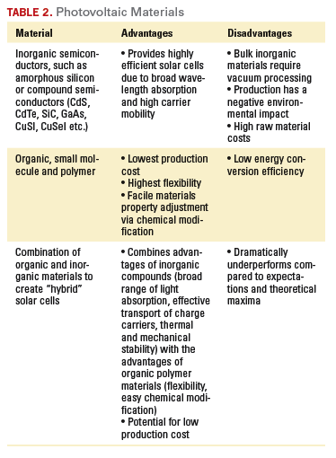
There are three major classes of photovoltaic materials (TABLE 2), and to differing degrees, they are all compatible with large-area processing and manufacturing platforms. However, organic photoactive materials are currently the most promising for large-area processing, as well as increased mechanical flexibility.

Two key technical attributes must be improved for broader commercialization of organic photovoltaic technology: efficiency/cost and stability/lifetime. Currently, the modest efficiencies and shorter lifetime of this technology confine it to the same cost-versus-performance curve as conventional first-generation crystalline silicon. A few of the efforts underway include:
- Efficiency/cost.
- Improved nanoscale morphology control of the organic photovoltaic bulk heterojunctions via self-assembly/self-organization.5
- Development of solution-processable and transparent conductive materials for flexible electrodes.
- More research into solution-processable hybrid organic-inorganic systems.
- Theoretical modeling of exciton physics at the bulk heterojunction interface.
- Development of polymers with optical harvesting properties (i.e., absorption of many photons by a dendritic polymer and fast intramolecular transfer of the excitons to a splitting site).
- Stability/lifetime.
- Fundamental studies to determine the origins of aging-based performance loss in bulk heterojunctions.
- Development of conjugated polymers and electron acceptors with higher stability.
- Development of low-cost, roll-to-roll encapsulation processes.
Sensors
Sensors represent another family of active devices that provide a near-term opportunity for large-area flexible electronics. In general, sensors under development today feature simple architectures for monitoring environmental and processing conditions. They include devices that change electrical or optical characteristics when subjected to an environmental change, such as temperature or humidity. Once observed, this information can be sent wirelessly (or via wireline) to control units for further action.
The potential for low-cost production, lower environmental impact during disposal and distributed sensing ad hoc systems make large-area flexible electronics a practical solution for many sensor applications, such as the first-generation classes of sensors discussed below.
M-commerce sensors. These devices detect when an upper or lower limit has been reached. Examples include pressure and strain color-changing indicators/sensors. These types of sensors do not require an energy source and have limited reliability attributes.
Ambient assisted-living sensors. These sensors detect the instance when an event has been triggered and have the ability to store that information in memory (e.g., temperature and humidity sensors). They require an energy source for operation (e.g., continuous calibration) and to store the triggered event in memory. This functionality provides for greater accuracy and reliability compared to M-commerce sensors. Also, the sensor design has wireless readout functionality based on industry standards.
E-health sensors. This class of sensors has the functionality to record the instance of a triggered event and sufficient memory to record a stream of historical data (e.g., medical sensors). These sensors provide high accuracy and repeatability functionality via an external power source. Most of these sensing solutions follow communications protocols that align with available near-field communication-enabled consumer electronics devices. Long-term, it is envisioned these types of sensor architectures will be embedded into objects to create a distributed ad hoc sensor network.
- The most often mentioned needs for commercialization and wide adoption of large-area flexible sensors are:
- Development of nano-material-based sensing devices with improved dynamic calibration to provide higher accuracy.
- Development of printed RAM for storing event history.
- Deployment of standardized readout technology and infrastructure.
- Development of disposable environmentally-preferred power sources for active sensing.
Numerous technology and infrastructure concerns must be addressed to bring large-area flexible electronics-based products to market. Functional inks, substrates, packaging and barriers, manufacturing platforms and processing equipment, testing and quality control, and standards are all areas where development is needed. The iNEMI Roadmap identifies the following gaps and showstoppers:
- Commercialization rate of materials, manufacturing/processing equipment and inline/offline characterization tools is slow and may not meet the cost/performance/utility demands to enable near-term product launches.
- Rate of development of large-area flexible electronic products must accelerate; otherwise, an opportunity may be created for a disruptor to commercialize an attribute-competitive product.
- Lack of design and simulation tools will slow the diffusion and acceptance of large-area electronics into the market.
- Lack of a well-developed supply chain and deep infrastructure will lead to products that are not cost competitive.
Despite the challenges to be addressed, large-area flexible electronic technologies will cause a paradigm shift in electronics. They will offer unlimited product design freedom, increased production throughput and lower cost for higher utility applications offering voice, video and data packaged in novel product form factors. Large-area electronics is an emerging field attracting increased attention within electronics, as demonstrated by greater participation in the 2009 Roadmap. Nearly twice as many people participated in the development of the 2009 chapter than the 2007 chapter. Participation from industry, academia and government labs was more diverse and included strong representation from international experts in graphic arts and semiconductors. Large-area flexible electronics is expected to be a growth segment over the next 10 years, offering attractive alternatives to “business as usual” electronics manufacturing. The 2009 iNEMI Roadmap is available at inemi.org/cms/roadmapping/roadmaporder.html. PCD&F
References
1. Nanomarkets, Printable Electronics: Roadmaps, Markets and Opportunities, Sept. 19, 2006, nanomarkets.net/products/prod_detail.cfm?prod=6&id=212.
2. IDTechEx, Organic Electronics Forecasts, Players, Opportunities 2005-2025, 2005, idtechex.com/products/en/view.asp?productcategoryid=82.
3. EInk Corp., eink.com/technology/howitworks.html.
4. Yanko Design, yankodesign.com/2008/01/04/high-tech-napkins/.
5. J.K. J. van Duren, et al, Adv. Func. Mat., vol. 14, no. 425, 2004.
Daniel Gamota is president of Printovate Inc. (printovate.com), and chair of the iNEMI Large-area Flexible Electronics TWG (Technology Working Group) for the 2009 Roadmap; This email address is being protected from spambots. You need JavaScript enabled to view it..


