A concurrent approach to design that considers manufacturing limitations will reduce errors, lower costs and improve time-to-market.
In today’s tense economic environment, companies that have not outsourced their PCB design value their designers as an integral project team member. As “first to market,” “quality first” and other positive expressions permeate your office, how can you, as a PCB designer, personally help your company’s short-term survival and long-term growth? One opportunity is by frequently using manufacturing analysis tools throughout the PCB design process to identify fabrication and assembly problems (especially after an ECO is introduced into the design). Eliminating these manufacturing problems as they are found will significantly improve your chances of shipping out the PCB design on or ahead of a project’s schedule, as well as minimizing initial in-house inspection of your build package at the fabrication and assembly houses.
The traditional PCB fabrication and EDA industries have adapted incrementally to the evolutionary development of printed circuit boards over the last few decades, without significant technological discontinuity. From the demands for high-end consumer products such as cellular telephones, to the medical field and reaching into Aero/Military products, all have revolutionized the PCB industry. No longer are the traditional design and fabrication methodologies sufficient. These types of products must be made faster, lighter and smaller, with less cost and higher quality. This high-tech density revolution has created the need for OEMs to embrace high density interconnect (HDI) technology.
However, the arrival of HDI circuits now represents a discontinuity in technology for PCB fabricators and the EDA industry—due to the sudden reductions in dimensional scale. HDI products go beyond the scope of traditional PCB fabrication processes. The changes in build architectures no longer match up with the database structures and the assumptions that were inherent in previous generations of CAD/CAM systems.
The One-Pass PCB Design Process
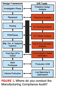
Extreme miniaturization trends place new demands on verification of designs such that manufacturing concerns must be addressed concurrently in the design flow. FIGURE 1 represents an ideal process for design while continually validating the designs’ manufacturability. This means that design for manufacturing verification must become a standard part of the design process – it’s YOUR job. In order to reduce the costs of building the designs and to meet the tightened time-to-production schedules, fabrication and assembly compliance checks must be made during placement, critical routing, power supply design and manufacturing documentation. The entire design process must integrate the requirements of the fabricator and assembler before launching a product into manufacturing.

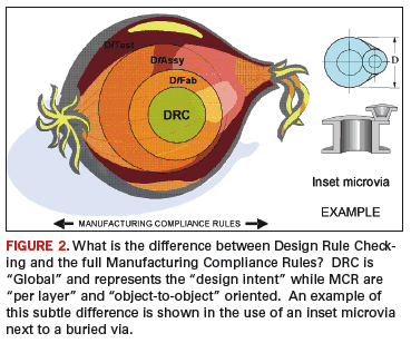
Design systems lay out circuits to defined rules (DRC); however, the systems adhering to these rules usually fail to represent the full extend of what constitutes manufacturability (manufacturing compliance). The purpose of reviewing the data package, in addition to reviewing the documented design constraints, is to confirm that the product can be produced at the manufacturing site and to the expected manufacturing yields. The analysis of the data describing the circuitry of the PCB to the manufacturing facility’s production capabilities is critical to the success of the product. FIGURE 2 shows that the typical DRC is a subset of manufacturing compliance rules (MCR), representing the difference between CAD, DRC and the full manufacturing compliance rules. DRC is an ideal process for design, but MRC continually validates the designs’ manufacturability.

Figure 2 illustrates that, like an onion, there are layers to manufacturing compliance. The example highlights this complexity: the inset via is a very useful HDI design feature but not all CAD systems will permit this feature, so the MRC must be sensitive to weather this is a designed feature or, an error in placement or routing.
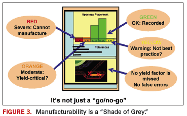
Once created, MCR files represent software specification that can be shared between design and manufacturing engineering as they collaborate throughout the entire product supply chain. Using the MCR inside the EDA environment, a designer can graphically see these manufacturing ranges, as seen in FIGURE 3. Partnering with the fabricator and assembler to understand these rules files will ensure that the manufacturing knowledge is built into the layout process. As described in the MCR, each analysis category must be driven by its own set of acceptability parameters to define the limits of yield compromise:

SEVERE: Unacceptable according to specifications
MODERATE: In the borderline zone, requiring judgment from a skilled engineer
WARNING: Acceptable but in a gray zone considered to be not best practice
OK: Acceptable according to specifications
With hundreds of discrete analysis functions and a range of different designs, interconnect technologies and manufacturing process options, an infrastructure is required to maintain all the variable rules and constraint parameters that have an impact on manufacturing yield, quality and cost. The MCR allows the engineer to capture all physical specifications and manufacturability constraints on demand. In the same way that Signal Integrity (SI) Analysis and Power Integrity (PI) Analysis can be driven by constraints captured during schematic input and permanently stored as part of the design file, these Manufacturing Compliances Constraints can be stored in the Constraint Editor. And like SI/PI analysis, models for MCR need to be established and maintained.
Typically, these MCRs are grouped into common categories such as:
- Proximity and clearances of signal traces
- Proximity and clearances of holes and vias
- Proximity and clearances of soldermask and legends
- Spacing and characteristics of signal traces
- Spacing and characteristics of planes and copper pours
- Spacing and characteristics of holes, vias and cutouts
- Spacing and characteristics of soldermask
- Spacing and characteristics of silkscreen and legends
- Spacing and characteristics of solderpaste
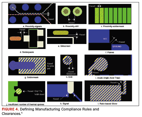
The organization and maintenance of these MCR files is shown in FIGURE 4. Figures 4a to 4l show some of the typical classification of these hazards.

Using Batch DFF as a Design Analysis Tool
The design rule checking results are reviewed against the PCB manufacturing capability matrix, with dispositions being made to the acceptability of violations. The PCB customer may be contacted regarding design violations, to correct and retransmit the design or to permit design changes to be performed by the PCB manufacturer. Additionally, the factors reviewed during the initial design review are revisited to confirm the results based on design actuals. If differences are noted, product yields and/or cost predictions may need to be altered. During this step of tooling, several concerns are uppermost in the fabricator’s mind: Does the board meet the intent of the design? Can it be built? Will it function as planned? Does it pass a master rule set? Can it be made cheaper or better? Is there component interconnectivity? Does the IPC-D-356 netlist show any shorted nets or broken nets? Were any multiple plane ties not happening? Did a design work-around fool the system––or allow intentional errors to slip through?
Bare-Board Analysis
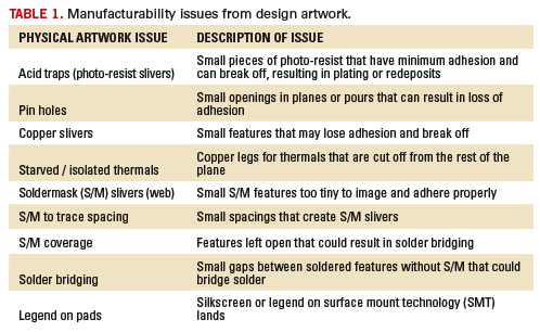
Several physical artwork problems are not discovered by design rule checking and are not the result of design rule violations. Nonetheless, these problems can affect the manufacturability of a board and its yield (as TABLE 1 describes and Figure 4.) Most modern CAM-tooling systems can correct these manufacturability issues, but it is better to find them during the layout process so that valuable time is saved! Thus, the manufacturing notes on the fabrication drawings should acknowledge this and allow for the fabricator to implement corrections. Other, less frequent, artwork errors discovered include embedded components and RF shapes.

Critical Inspection Points – What To Focus On
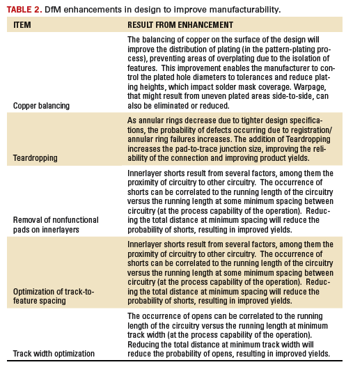
The manufacturability of the PCB can be improved through design enhancements. Many of the enhancements can be performed on CAD systems (or through specialized post-CAD software); other enhancements can be performed at the manufacturing site. Ideally, all design enhancements would be performed at the design site to maintain the consistency of products from multiple manufacturers. Some of the DFM enhancements can impact the CAD system’s capability to provide further design changes. Specifically, the optimization of track-to-feature spacing could result in blocked routing channels, preventing an autorouter from performing. The TABLE 2 shows typical DFM enhancements.

When it is appropriate to conduct various manufacturing compliance analysis, they are best performed after:
- Placement of components.
- Routing and simulation with signal integrity constraints.
- Plane pours and simulation with power integrity constraints.
- In-Circuit Testpoints, silkscreen, legend and solder-paste and any other manufacturing documentation and DfT analysis.
- Final “sign-off” and before the package is sent out for fabrication.
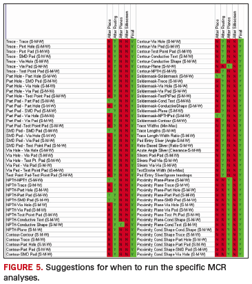
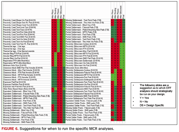
FIGURE 5 and FIGURE 6 provide a suggestion for when to run specific batch DFF analyses. Since the MCR can be saved and stored, this is not a difficult task. Any hazard discovered can then be corrected, and this is “one less” that can result in missing critical schedules.


Conclusion
Implementing a concurrent approach to design, with manufacturing always in mind, will reduce errors, costs and time-to-volume-production. One of the keys to ensuring success is using manufacturing supplied compliance criteria in the design environment. The implementation of new Manufacturing Compliance software in the supply chain will increase effective communication between the OEM, fabricator and EMS. Additionally, it ensures the design processes match the needs of multiple manufacturing suppliers, which means that the manufacturing output is “correct by construction” before it leaves the layout engineer’s desktop. This in turn eliminates the downstream design iterations. PCD&F
REFERENCE
1. Holden Happy, “Manufacturing Information, Documentation, and Transfer Including CAM Tooling for Fab and Assembly,” Printed Circuit Handbook-Sixth Edition, pgs. 20.1 -20.32, McGraw-Hill, 2008.
Happy Holden is senior technologist with Mentor Graphics; This email address is being protected from spambots. You need JavaScript enabled to view it.. Daniel Smith is technical instructor with Mentor Graphics; This email address is being protected from spambots. You need JavaScript enabled to view it..


