Embedded active technology offers advantages in reduced parasitics and form factors, but thermal dissipation and rework issues are delaying commercialization.
Embedding integrated circuits (IC) within a multilayer package dates back to the work of Gene Weiner at MIT’s Lincoln Laboratory in 1950. The team placed devices within resin and routed interconnections by mechanical drilling.1 However, the leapfrog work is credited to General Electric. In the early 1990s, the company accomplished the real embodiment of chips in a multilayer package.2 Since the inception of GE’s "chip first" process, several approaches have been undertaken in embedding chips into polymer and other thin core matrices. Such innovations can be encompassed by three major categories: cavity formation to the size or volume of the chip, lamination similar to the LTCC process adopted in ceramics with the chip within the multilayer laminated sheets and over-molding upon placement of the chips.3 Besides reduction in thickness, another key advantage in embedding actives is the decreased interconnect length. An analysis of parasitics in different package configurations was conducted by Daum2 at GE. Results showed that HDI with embedded components and actives could lead to a significant reduction in parasitics.2
In recent years, Liquid Crystal Polymer (LCP) has received attention as a high-frequency substrate material. LCP has low dielectric constant (~2.97), low dielectric loss and temperature stability up to 125ËšC across a wide frequency range up to 110 GHz.4-6 The coefficient of thermal expansion (CTE) of LCP can be engineered to match that of copper, silicon or GaAs. The availability of two types of LCP substrates with different melting temperatures makes it possible to realize multi-layer architectures. LCP is uniquely positioned at a frequency band where conventional organic dielectrics, such as FR 4, degrade in performance (at around 5 GHz). Nevertheless, to date, the major constraint for the commercialization of LCP has been its processability, such as surface treatment, handling of thin flexible films and layer-to-layer registration and via formation and plating. These issues have been addressed by several academic7-8 and industrial organizations, such as Endicott Interconnect Technologies9 and Foster-Miller Inc.10
Embedded devices in LCP have been realized by the lamination process with micro-machined cavities, as well as by the molding process with a liquid polymer. A combined path in embedding chips and passives and enhancing thermal performance of the embedded IC in a flex circuitry was first reported by Torikka11 using LCP and liquid Benzocyclobutene (BCB). BCB provides the lowest dielectric loss (Dk = 0.0008) among the polymers. The key advantages in combined solid LCP/liquid BCB processes are thermal cooling from the back of the chip and feasibility of coreless packaging.12
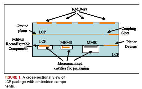
Comprehensive research and prototypes have been published leading to the realization of embedded RF components and devices in all LCP packages.4-6 A conceptual layout of an all-LCP organic package with micro-machined cavities to host actives such as amplifiers and oscillators, discrete components and MEMS is depicted in FIGURE 1. The following sections show examples of embedded ICs in single and multilayer LCP.

Embedded VCO
A mm-wave 36 GHz SiGe voltage controlled oscillator was embedded in a laser-cut cavity13 and packaged within core LCP while maintaining a high performance profile (FIGURE 2). Photolithography and copper etching made the transmission lines on the LCP. A cavity that matches the lateral dimension of the VCO was laser cut using a KrF 248 nm UV Excimer laser. The laser cut LCP was then mounted on Si wafer. The VCO was dropped through the precut window and secured to the carrier Si substrate (FIGURE 2A). The connections to the transmission lines were made by wire bonding (FIGURE 2B). Measurements of both wafer-level and package-level oscillators were done on an Agilent E4446A spectrum analyzer. A plot of the output spectrum of the packaged oscillator, with respect to the unpackaged performance, is depicted in FIGURE 2C. The increased parasitics of the packaged part causes an additional 1.9% shift in oscillation frequency. The output power of the packaged part is 3 dB down from that of the unpackaged part (FIGURE 2C). Measurements after packaging showed a figure of merit 13 dB down from the on-chip measurements. Much of this degradation in oscillator performance is expected due to the wire bond connections.

Three-dimensional Phased Array with RF MEMS switches and LNA
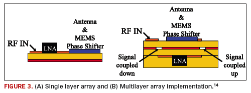
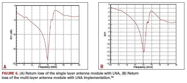
A fully integrated phased array antenna with radio frequency micro-electro-mechanical systems (RF MEMS) switches on a flexible, organic substrate was demonstrated above 10 GHz for use in a NASA Earth observing satellite system.14 The fully integrated array consists of a MMIC LNA, MEMS phase shifter, RF power distribution network, biasing circuits and antenna arrays. In this 3D prototype, two antenna arrays are compared; the first is implemented using a single-layer and the second with a multi-layer LCP. Both implementations are capable of 12 degrees of beam steering. The design frequency was 14 GHz and the measured return loss was greater than 12 dB for both implementations. The use of an LNA allowed for a much higher radiated power level. FIGURE 3 shows the conceptual drawing of single and more compact multi-layer approaches.

The module operates by receiving an RF signal at 14GHz. The signal is amplified by an LNA and then fed to a pair of one-bit MEMS phase shifters. If the phase shifters are in phase, the antenna array radiates perpendicular to the substrate. If the phase shifters are out of phase, the radiation is steered left or right – depending on the length of the phase path.
Single-Layer Module
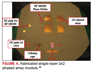
The antenna array was fabricated on a 3-inch diameter circle that was precisely cut using a CO2 laser. An electron beam evaporator was used to deposit a Ti-Au layer. A silicon nitride layer was deposited using PECVD and etched using an RIE. A 2-µm thick sacrificial photo resist layer was patterned and hard baked. An electron beam evaporator was used again to deposit a 200A-2000A-200A Ti-Au-Ti layer. Electroplating was used to increase the gold thickness of the antennas and MEMS bridges to 1.5 µm. The sacrificial photoresist layer was removed using a stripping agent and dried with a CO2 critical point dryer. The DC bias lines for the capacitive RF MEMS switches were evaporated with the first seed layer and were not plated. The ground and bias pads for integration of the MMIC LNA were added at the same time as the MEMS to prevent any additional process steps. Once the MEMS were released, the LNA and off-chip capacitors were mounted onto the sample using silver epoxy and were wire bonded to connect the LNA to the DC bias and RF signal lines. FIGURE 4 shows the fabricated single layer module.

Multilayer Module
Implementing a multilayer configuration is much more challenging than a single-layer configuration because the approach requires multilayer alignment, device packaging, substrate bonding, fabrication on two sides of a substrate and a method for transmitting the data across layers.
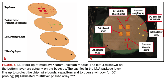
The top substrate was fabricated in the same way as the single-layer approach without the LNA. On the backside of the top substrate, the metal layer is etched to provide the window for aperture coupling. The final fabrication stackup is shown in FIGURE 5A. There are four main layers. The top layer has the RF input, MEMS phase shifters and phased array. The bottom layer has the LNA and off-chip capacitors. The LNA package layer has laser micro-machined cavities that protect the LNA, wire bonds and off-chip capacitors. It also provides a window for accessing the LNA DC bias pads. The LNA cap layer covers the cavities to protect the components inside. The DC bias for the LNA is accessed on the backside of the antenna to minimize interference of the DC biasing wires with the antenna. The LNA was centered directly under the 2x2 array. Before the system was assembled, all of the layers were fabricated independently and then bonded together. The fabricated multi-layer antenna array is shown in FIGURE 5B.

The multilayer module (FIGURE 5B) is 25% smaller in size due to the placement of the LNA in the interior layer. Another advantage of the multi-layer module is that the antennas can be effectively shielded, thereby preventing radiation from other components. However, in this prototype, the multi-layer implementation shows more loss due to longer RF signal length and aperature coupling. FIGURE 6A shows the measured return loss of the single layer antenna with LNA, and FIGURE 6B shows the multilayer antenna array with the LNA. Using thick, highly conductive metal can minimize line loss. Properly simulating the device and having good alignment accuracy during fabrication can minimize the aperture coupling loss. The use of metal-filled vias could also reduce the loss.

An embedded active is a viable technology offering advantages in reduced parasitics and form factors and has been proven to be technologically feasible. However, thermal dissipation and reworkability issues are still considered bottlenecks for commercialization. LCP has been proven to be a promising dielectric for multilayer 3D packages with embedded actives without significant degradation of RF performance of the packaged chips in the mm-wave frequencies. PCD&F
REFERENCES
1. J. Fjelstad, “A brief history of embedded device technology,” Global SMT and Packaging Magazine, Issue 8.3, March 2008.
2. W. Daum, W. Burdick and R. Fillion, “Overlay high-density interconnect: a chips-first multichip module technology,” Computer, vol 26, issue 11, 1993, pp. 23-29.
3. D. Fritz, “Coming-Embedded Active Components, How Does IPC Respond,” IPC TAEC Meeting, Minnapolis, October, 2004 [Source: Japan Jisso Technology Roadmap, 2003 Edition, JEITA].
4. D. Thompson, O. Tantot, H. Jallageas, G. Ponchak, M. Tentzeris and J. Papapolymerou, “Characterization of Liquid Crystal Polymer (LCP) material and transmission lines on LCP substrates from 30 to 110 GHz,” IEEE Transactions on Microwave Theory and Techniques, Vol. 52, No. 4, April 2004, pgs. 1343–1352.
5. D. Thompson, M. Tentzeris and J. Papapolymerou, “Experimental analysis of the water absorption effects on RF mm-wave active/passives circuits packaged in multi-layer organic substrate,” IEEE Transactions on Advanced Packaging, Vol 30, 2007, pgs. 551-557.
6. N. Kingsley, “Liquid crystal polymer: Enabling next generation conformal and multi-layer electronics,” Microwave Journal, 2008, pgs. 188-200.
7. X. Duo, L. Zheng and H. Tenhunen, “Design and implementation of a 5 GHz RF receiver in LCP based system-on-package with embedded chip technology,” IEEE Electronic Components and Technology Conference, 2003, pgs. 51-54.
8. M. Chen, A.V. Pham, Chris Kapusta, J. Iannotti, W. Kornrumpf and J. Maciel, IEEE Transactions on Microwave Theory and Techniques, Vol 56, No 4, April 2008, pgs. 952-958.
9. M. Rowlands and R. Das, “Manufacture and ultrahigh performance of an LCP based Z-interconnect flip chip package,” IEEE ECTC 2008, pgs. 1362-1367.
10. R. Dean, J. Weller, J. Bozack, C. Rodekohr, M. Bozach, B. Farrell,L. Jauniskis, J. Ting, D. Edell and J. Hetke “Realization of ultra fine pitch traces on LCP,” IEEE Transactions on Component and Packaging Technologies, Vol 31, No 2, June 2008, pgs. 315-321.
11. T. Torikka, D. Xinzhong, Z. Li-Rong, E. Tjukanoff and H. Tenhunen, “Chip-package co-design of a concurrent LNA in system-on-package for multi-band radio applications,” Electronic Packaging and Technology Conference, Volume 2, June 2004, pgs. 1687 – 1692.
12. S. K. Bhattacharya, M. Tentzeris, L. Yang, S. Basat and A. Rida “Flexible LCP and paper-based substrates with embedded actives, passives, and RFIDs,” Polytronics 2007, Tokyo, Japan, January 2007.
13. C. Patterson, S. Horst, S. Bhattacharya, J. Papapolymerou and J. Cressler, “Low cost organic packaging for silicon based mm-wave wireless systems,” European Microwave Conference, Amsterdam, October, 2008.
14. N. Kingsley, G. Ponchak and J. Papapolymerou, “Reconfigurable RF MEMS phased array antenna integrated within a liquid crystal polymer,” IEEE Transactions of Antennas and Propagation, Vol 56, No 1, January 2008, pgs. 108-118.
15. N. Kingsley, “Development of Miniature, Multilayer, Integrated, Reconfigurable RF MEMS Communication Module on Liquid Crystal Polymer (LCP) Substrate,” Ph.D. Dissertation, Georgia Institute of Technology, 2007.
Swapan K. Bhattacharya, Nicolas Kingsley, Chad Patterson and John Papapolymerou are associated with the School of Electrical and Computer Engineering, Georgia Institute of Technology. Atlanta, GA 30332, USA. Swapan K. Bhattacharya can be reached at This email address is being protected from spambots. You need JavaScript enabled to view it..


