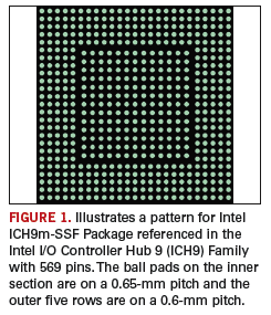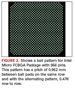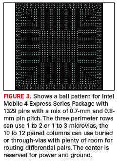
PCB footprints for mobile chipsets.
Although I am considered an expert in my field, and I am well- learned in many other areas, in the context of all possible knowledge, my ignorance is still infinite. With technology, there are so many avenues to pursue that we gladly rely upon others to walk the unknown paths. Our combined observations, insights and creativity magically result in progress towards faster, cheaper and better products with a goal to lift the standard of living for all mankind — at least from my optimistic point of view.
Researching BGA routing challenges has been an interesting endeavor and communicating my discoveries has allowed me the privilege of knowing that I, too, have made some small contribution to the advancement of PCB design. What pleases me even more is meeting people in this industry who tell me of their ideas, struggles and successes in their own pursuits.
During the past year, I have spent much of my time with PCB designers discussing the challenges of routing large dense BGAs. At the beginning of the year, when addressing an audience, I would ask two questions: how many used BGAs with over 1500 pins; and how many were either using High Density Interconnect (HDI) or evaluating it. A year ago, the results were along the lines of 20% and 25% respectively. During the past few months, the response has risen to about 30% and 75%. Although my ad hoc polling is of no scientific value, the results are in line with some trends I have observed during my meetings with designers.
The movement to HDI fabrication has increased significantly, driven primarily by the mobile and handheld market and, more importantly, due to the use of fine-pitch BGAs, meant for the mobile market, on other products. What appears to be driving the adoption of HDI is not the 1500-pin to 2000-pin BGA at 1.0 mm pin-pitch; but rather, it is the 400-pin to 600-pin BGA at 0.6 mm pin-pitch or smaller.

Often, I speak of a threshold that will force these designs into HDI. This threshold will be crossed when the 0.8-mm pitch BGA with 2000 pins arrives and multiple instances are required on one design, for example, on network cards or emulation cards. Using drilled through-vias will not be practical because it will result in too many layers. This threshold has not been crossed yet. Large pin-count FPGAs and ASICs are still being packaged with a 1.0-mm pitch.

While the large pin-count packages have remained relatively stable, the fine-pitch (<0.8mm) BGAs with over 400 pins have arrived this year and are causing trouble for PCB designers. Most of the questions I get are along the lines of, “I have this 500-pin BGA with a 0.6-mm pitch. What kind of fanout pattern can you recommend? Oh, and did I mention we are required to use through-vias?” Invariably, early in the design cycle, someone made a decision to use a fine-pitch BGA meant for a handheld device on a larger computer board. Last month’s BGA Bulletin column is focused on solutions for those situations.

I continue to hunt the Internet for new BGA packages. Most recently, Intel has published datasheets for mobile chipsets that include some very interesting ball patterns. FIGURES 1, 2 and 3 illustrate the PCB footprints I made for those devices. PCD&F
Charles Pfeil is an engineering director for Mentor Graphics, Systems Design Division. Email: This email address is being protected from spambots. You need JavaScript enabled to view it.. At www.mentor.com/go/bga you can obtain a copy of Charles’ book, “BGA Breakouts & Routing”.


