Communication, documentation and teamwork between suppliers reduces the risk and increases the benefits of outsourcing.
The growth of portable wireless products and related consumer electronics is fueling a major outsourcing effort toward Asia. Most OEMs (original equipment manufacturers) are partnering with CMs (contract manufacturers) in Asia to outsource key operations such as board design, fabrication, surface-mount assembly and procurement to maintain profitability and a competitive edge.
Outsourcing can offer OEMs significant advantages in maintaining a healthy bottom line, including reduced capital risks, increased access to current technologies and reduced time to market. Outsourcing also allows CMs and EMS (electronic manufacturing services) companies to subcontract the work that does not fit their core competencies, so that they can diversify their products.
Outsourcing with strategic partners is more important for OEMs dealing with lead-free migration since this new requirement brings many challenges for the PCB fab and assembly industries. With new high Tg (glass transition temperature) laminates, new lead-free alloys, rework processes, moisture sensitivity and other issues, the entire manufacturing process requires careful evaluation of new laminate materials to balance component layout and optimization of reflow profiles to minimize damage to PCBs. This is especially critical for thin PCBs (less than 0.1 mm) used in cell phones and other portable products, and PCBs based on build-up microvia technologies.
The handheld wireless product marketplace demands products that are small, thin, low-cost and lightweight with improved user interfaces. In addition, the convergence of handheld wireless phones with palmtop computers and Internet accessibility is accelerating the need for functional circuits designed with miniaturized, low-cost technology.
Outsourced PCBs from Asia are becoming more of a viable option for OEMs involved in high-volume manufacturing. Proper evaluation and qualification of these facilities is critical for assembly reliability.
There are critical aspects in the qualification of PCBs. Qualification efforts especially for HDI (high-density interconnect)1 and ALIVH (any layer inner via hole) PCBs2 procured from Asian fabricators in China, Taiwan, Korea and Japan need specific characterization. Quality systems audit results, PCB evaluation, acceptance criteria, DPPM (defective parts per million) review and reliability testing need to be evaluated. Additionally, strategies for overcoming cultural differences, communication, conflict resolution, and building supplier and customer relationships have a high level of importance.
High-volume surface-mount assembly production requires careful evaluation since as assembly yields depend heavily on good quality PCBs, solder paste print processes and oven reflow profiles. This has become more critical in lead-free reflow due to higher peak temperatures and narrow process windows. Proper storage, handling control in the supply chain and production process control is necessary for good yield and reliability. DPPM reduction efforts must focus not only on the manufacturing processes but also on overcoming many cultural, communication and interpretation differences.
Supplier Audit and Qualification
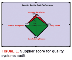
The qualification effort required a factory and warehouse visit, and conducting a quality systems audit of the PCB manufacturing process. Critical items such as ISO 9001-2000 certification, a capabilities survey, staff training and certification, the eight discipline process, design management, and materials controls were reviewed. Based on this review, a ranking was provided for four major categories: customer satisfaction, manufacturing process, materials management and quality system. The supplier was then certified for production based on a minimum score of 90% or above as shown in Figure 1.

Most manufacturers in Asia have some percentage of their operations outsourced. It is important to understand the manufacturing process of your product or technology, and to also survey any subcontract operations during the audit since process controls implemented there also affect the end product. In this case, all action items generated from the audit were closed within five working days. It is also important to follow up with annual quality audits.
Product Qualification. The board assembly process that qualified used a double-sided, surface-mount assembly soldering of BGA (ball grid array) packages, connectors, chip resistors, capacitors, diodes and other components. Assembly reflow took place using convection air at a peak temperature of 244°C. The assembly solder paste used was SAC 305 (tin/silver/copper) no-clean version.3
Cross-sections were performed on BGA packages and other components to evaluate the quality of the solder joints and ensure compliance to IPC 610 – Rev D for leaded packages and IPC 7095 for BGA packages. Microvia integrity was also evaluated with cross-sectional analysis. Cross-sections showed acceptable solder joints and no degradation of the microvias.3,4
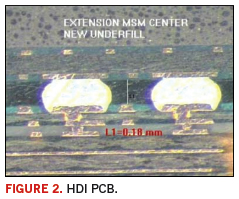
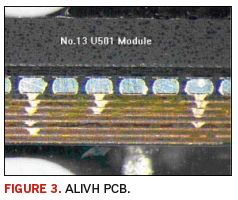
The qualification process was conducted using product build for a phone program and cross-sectional analysis, and reliability testing per IPC 9701.5 Temperature and humidity tests were conducted at 85°C at 85% relative humidity for 500 hours, and thermal shock testing was conducted from –25°C to +125°C at 20 minute dwell for 500 cycles. Figure 2 shows cross-sections for HDI board assembly post reflow, and Figure 3 shows ALIVH PCB assembly post reflow.


Rework Process
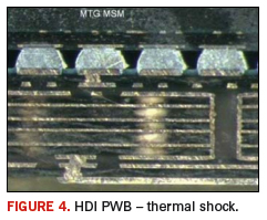
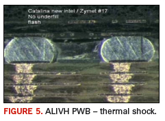
Surface-mount packages were reworked using hot-air soldering tools, and BGA packages were reworked with hot air using controlled ramp/soak profile. The main concern was damage to microvia connections and PCB pads during component removal and reattach. Component rework was performed two times on the leaded packages and one time on the BGAs. All packages survived rework. There was no damage to PCB pads or blistering of the solder mask during rework. No damage was seen on microvia connections. Figures 4 and 5 show cross-sections of HDI and ALIVH PCB post rework after 500 thermal shock cycles.


Production DPPM Issues
There were two types of production rejects. Cosmetic rejects were lots rejected at the incoming IQC inspection and functional rejects where the lots were rejected post reflow (after surface-mount assembly) and during board-level electrical test.
Cosmetic Rejects. Incoming inspection was performed using IPC 600 Rev G. There were many product rejections due to incorrect paperwork, scratches, exposed copper and more. A meeting was held with suppliers and CMs to address the problems; after which, suppliers put a plan in place to address scratches and exposed copper, reducing the errors going to the CM. The Kyocera Wireless Corp. (KWC) team audited the suppliers for corrective action. There were several other process flow and material handling issues that had to be resolved to minimize PCB problems at surface-mount production.
Prior to assembly outsourcing, PCBs were shipped from supplier locations to KWC in San Diego, CA, and immediately utilized for production, so staging and storage was minimal. This situation changed when surface-mount factory operations moved to contract manufacturing in China. Due to customs requirements, all parts shipped to China must go through customs in Hong Kong and then are staged in a warehouse facility until they are ready to move to the CM’s warehouse, resulting in increased staging time and handling for PCBs. Suppliers were required to improve the packaging from standard plastic bags to specialized seamless bags that were vacuum sealed with a desiccant inside. This required some changes in PCB packaging, but in the long run resulted in higher reliability. The warehouse audits were conducted to ensure that temperature was maintained at 22ºC +/- 5ºC with humidity less than 60%. Particular attention was given to storage during the summer months when heat and humidity were very high in this geographic area.
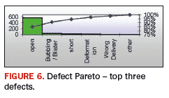
Functional Rejects. The majority of the defects after reflow were classified into three major categories: opens, delamination and shorts. This required a review of handling and test operations at CMs and process controls at suppliers. The corrective action began with compiling defect data and meetings with the supplier and the CM. This was followed up with storage and handling audits to ensure that corrective actions were being executed properly. Fabricators implemented corrective actions in the PCB packaging area by changing the bake cycle to 120°C for four hours prior to dry packaging. The CM implemented corrective actions at IQC by resealing all packages opened for inspection before returning to storage. On the production floor, packages were only opened just prior to loading on the assembly line, and all opened packages were stored in dry boxes. Reflow assembly time was controlled within 48 hours. Warehouse corrective actions were implemented to store PCBs in a controlled temperature/humidity portion of the warehouse, and FIFO (first in, first out) was enforced.
To address delamination issues, PCB suppliers conducted a design of experiments (DOE) with their material suppliers to get a better understanding in processing high Tg laminates. Circuit trace "opens" issues were addressed by implementing controls in the electroless plating process and various other plating and cleaning bath parameters and controls. Additionally, controls were implemented in the hot-air rework process at the CM since some of the "opens" issues were occurring after rework. Proper training of rework operators, controlled distance of hot air nozzles and airflow, and ongoing audits further helped to lower DPPM for open-circuit defects. The issue of short circuits was addressed by controlling contamination in the PCB exposure, develop and etching process, and implementing proper sampling frequency to minimize the escape to the CM.
All of these combined efforts have helped reduce the DPPM post reflow and minimize scrap cost.
Communication Strategies
When switching from in-house manufacturing to an overseas manufacturer, a number of time, distance and translation difficulties get added to resolving daily line issues. As an OEM, it is essential to keep your documentation correct and updated because misinformation can cause yield loss, a delay in shipments to the customer and chargebacks to an OEM.
A PCB is a complex commodity. When parts are rejected, it requires a good understanding of the PCB manufacturing process, the acceptance criteria, failure analysis of defects and root cause determination.
Since the CM did not have a very knowledgeable PCB team, OEM component engineers had to mediate when rejections occurred. This helped both sides (the CM and PCB suppliers) understand the defects and work toward an improvement plan.
The first step was holding a meeting of suppliers and the CM to understand the CM’s IQC spec and acceptance criteria. Simple lot rejects caused by incorrect paperwork, labeling, cross-outs and other issues were eliminated after an understanding of IQC specs. The lot acceptance rate at IQC improved to 100% within six months.
This process was followed up with monthly DPPM data to suppliers and tele-conferences. For major problems, up to five failed samples were sent to the supplier for failure analysis. Additionally, each quarter, all parties met at the CM facility and reviewed DPPM and defects. This gave suppliers a chance to meet the CM team and understand the assembly operations and part movement procedures. Supplier teams reviewed the failure analysis data, and corrective action plans were defined.
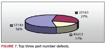
To assist the supplier teams in finding the root causes of defects, specific information was provided, rather than general DPPM bar charts. DPPM data was broken down into the top three defects and top three part numbers where problems occurred to enable the suppliers to first “root cause” the major issues and minimize their impact on production. An example is shown in Figures 6 and 7.


Conflict Resolution
The differences in operations, parts management, chargeback system and language at the CM did result in conflicts concerning scrap charges. In these cases, the OEM had to intervene and ensure that a fair resolution of the chargeback was taking place. The failure analysis was evaluated to ensure that the correct root cause was determined. If it was a supplier fabrication issue, the supplier was charged. If it was a process-induced defect such as uncontrolled rework, the CM was charged. If both parties contributed, the charge was split.
Training/Knowledge Base
The labor force in the CM factory was primarily a very young group with not a lot of experience or training time. Proper monitoring of training levels is important for good yield and product reliability. This is also essential due to employee turnover. Tight control should be maintained over all process changes, engineering change orders (ECOs), manufacturing change orders (MCOs), etc. OEM-led training sessions in product handling, test, storage and inspection have also improved yields.
Conclusion
Outsourcing assembly operations gives OEMs the advantage of high-volume manufacturing capacity, massive database systems and corporate direction. However, it also brings many new challenges in cultural differences, communication barriers and skill levels that we have not experienced with U.S. PCB manufacturing. Clear, concise communication, documentation, patience and teamwork between suppliers and CMs are just a few ways to ensure success. PCD&F
REFERENCES
1 Microvias for Low Cost, High Density Interconnect. John H. Lau, S. W. Ricky Lee.
2 The Progress of the ALIVH Substrate. Daizo A., Yoshihiro T., Tadashi N., Fumio E.
3 IPC A-610 Rev D – Acceptability of Electronic Assemblies.
4 IPC 7095 – Design and Assembly Process Implementation for BGAs.
5 IPC 9701 – Performance Test Methods and Qualification Requirements of Surface Mount Solder Attachments.
6 “Control and Stability in Lead Free Reflow,” SMT. R. Burke, Sept. 2006, Vol. 20, No. 9, pp. 24 - 26, 28.
Mumtaz Y. Bora is a principal quality engineer at Kyocera Wireless Corp. and can be reached at This email address is being protected from spambots. You need JavaScript enabled to view it..


