New collaborative systems connect designers and extend their reach beyond the PCB to other disciplines, enhancing the product development cycle.
Dramatic changes have affected the electronics industry in the past few years and changes continue. Competition is steeper. Emerging countries once known for inexpensive manufacturing are now mainstream suppliers of high-end competitive products. Electronic companies once vertically organized from design through manufacturing now find themselves not only outsourcing manufacturing but also portions of their product design. PCB fabrication technologies are rapidly advancing. All of this puts companies on steep learning, technology adoption, and re-organization curves that require the use of more sophisticated and costly EDA design solutions. Such is the price of staying competitive.
Regardless of the industry segment (telecom, consumer, automotive, industrial, and even military and aerospace), there are common business needs expressed by all electronics companies as they strive to survive. The first need is to meet ever decreasing time-to-market goals. Especially important in the consumer industry where product life cycles are measured in months, the company’s ability to hit a short market window and charge premium pricing for their new product makes the difference between profit and loss. Witness the iPhone, where just months after the first introduction, the price of a unit was reduced by hundreds of dollars and Apple’s inability to ramp production to full volume in the first months cost millions in profit. Even in the non-consumer automotive industries, time-to-market is becoming an important business requirement and driver.
The second common need and driver in today’s competitive world is reduced development costs. Making designers more productive and adding efficiencies to the total product development process all affect the bottom line and enables companies to produce more profitable products with their limited resources. Removing wasted efforts and enabling designers to focus on the product — not how to use design tools — gives them more time to innovate, which leads to the third business need.
That third need is to produce more competitive products (more functionality in smaller spaces at lower product cost). Unfortunately, this is often at odds with the first two business requirments. More competitive products often require the use of advanced IC, FPGA, and PCB fabrication technologies, which adds to the complexity of the design process.
Industry Trends Increase Design Complexity
We have all heard the expression, “the world is going global,” and this really applies to the electronics industry. Not all that long ago, the design and manufacture of electronic products of any significant complexity were performed in the U.S. or Europe. In recent years, China ramped up its manufacturing capabilities so that it can now produce equally sophisticated products. Companies in the U.S. and Europe now routinely outsource much of their manufacturing to facilities overseas. Following the manufacturing, design talent in countries like China is also rapidly improving and many companies are outsourcing all or part of their designs as well. So “going global” means that not only must companies compete with countries like China, but also leverage the talent in China while protecting internal IP, managing an increasingly complex infrastructure, and creating differentiated products.
Creating differentiated products products often requires the use of the most advanced technologies. IC and FPGA offerings continue to advance following Moore’s law. Data transfer rates in the multi-gigabit per second range and pin counts in the thousands per package create PCB design problems. Implementing these high-speed, high-density components requires the use of advanced PCB fabrication technologies like HDI and microvias, and embedded passives in order to fit and route all the components onto the PCB. Meeting interconnect delay signal integrity constraints adds to the complexity, as many designs now have 50 to 80% high-speed nets.
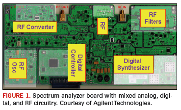
Another trend we see rapidly emerging in many industries is the use of RF circuitry incorporated into an analog and digital board. Long present in the military and aerospace industry, this technology is now prevalent in wireless telecom, automotive, medical, industrial, and consumer goods. These system designs may contain several sections of RF that are tightly packed into sections of an analog or digital board, as illustrated in Figure 1.

PCB Design – The Center of the Universe?
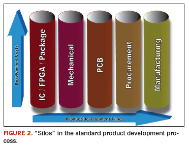
Most PCB designers tend to focus solely on the PCB design problems and processes, but product design requires much more than the PCB. To meet our companies’ business needs we must consider productivity and process efficiencies in the complete product development process. In many companies, organizational boundaries and lack of communication capabilities between the various disciplines creates “silos” (Figure 2) that tend to isolate potential teams and create development process inefficiencies.

A company’s aggressive business needs requires product developers to meet not only higher productivity goals within all of the design and manufacturing disciplines, but also improve efficiency between all of the design and manufacturing disciplines. This in the face of increasing complexities in the product designs itself, and the fact that these various organizations may be spread around the country or even the world.
Some of the burden falls to EDA suppliers like Mentor Graphics who must not only provide incremental improvements in their functionality, but also supply innovative new technologies that enable quantum leaps in productivity and process efficiency. Some of these “leaps” must extend outside of the PCB design domain and form bridges (or a collaborations) between PCB design and the other disciplines in the development process.
Collaboration – Intellectual Property Management and Access. A company’s intellectual property (IP) comes in many forms including component libraries, reusable design data, design-in-progress data, constraints (high speed and manufacturing) and design intent, design and manufacturing best practices, preferred tool flows, etc. IP is of little use unless it can be managed and made available to all members of the design team on a timely basis. Electronic CAD (ECAD) data management systems integrated with PLM and ERP systems must provide the necessary management of and access to the IP.
Collaboration – Between ECAD Disciplines. Most competitive designs contain one or more high-speed, high-density ICs or FPGAs. As previously noted, an increasing number of designs now contain a mixture of RF incorporated into analog and digital sections of a PCB. Providing the ability for these various disciplines to collaborate on a product design can significantly improve the productivity of the individual designers, and also produce a more competitive product. For example, being able to assign the I/O pins on an FPGA in the context of the PCB (versus independently without consideration for PCB interconnect) can significantly reduce routing lengths, improve performance, reduce PCB designer routing time, and can even reduce PCB cost by reducing the number of board layers.
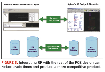
In the past, RF design was performed independently of the PCB design. Recently, RF design and simulation specialty products have been closely integrated with analog and digital design systems to create a collaborative team environment, as shown in Figure 3.

Collaboration – Beyond ECAD. Extending collaboration into other disciplines beyond electronic design can also make a big difference in process efficiency. An example is to create a collaborative environment where the ECAD and MCAD designers communicate during the design process electronically rather than using paper. The typical method of paper communication to proposed changes, either from the ECAD engineer or the MCAD designer, is a long, cumbersome, and error prone process. By implementing collaboration tools, when a change is proposed, the change can be communicated to the other disciplines who have the opportunity to view the proposal in a familiar environment (viewed in a typical PCB layout tool or mechanical 3-D tool respectively), comment, offer a counter proposal or approve the change, and then have that communicated back to the proposing party. All of this, in real time, represents a significant improvement over paper communication methods.
Collaboration between ECAD and the rest of the enterprise throughout the design process can also significantly affect the product development process efficiency, and may even mean the difference between a profitable and non-profitable product. Prime examples include real-time collaboration between ECAD, manufacturing and procurement. For example, electronically communicating a proposed PCB design change (a different component) to procurement and manufacturing give them the opportunity to review the proposal for volume purchase, price, and manufacturability in real time. This is especially important when design and manufacturing may take place at different locations around the world.
The Cost of Being Competitive
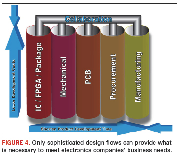
All of the trends and technology discussed lead to one conclusion: ECAD systems that provide this level of design capabilities are highly sophisticated. They are tightly integrated flows with IP management and integrated into corporate systems. They contain design capabilities for the most advanced technologies with easy-to-use human interfaces. They extend beyond PCB design and provide collaboration with other disciplines within ECAD, and on to other product development and manufacturing organizations. Collaboration connects the silos together, as illustrated in Figure 4.

These sophisticated design flows require extensive R&D investment to develop, deliver to users, and support. These systems do not come cheap, but electronic companies are switching from commodity PCB design systems to ones that can provide this level of product development support are realizing that investing in these systems puts them at a competitive advantage. Companies are also investing in the infrastructure support and training required to operate these systems. We even see countries like China that previously survived on low-end design systems now switching to systems containing the most innovative technologies available. Be cautious, U.S., Japan and Europe! Competition will only get tougher. PCD&F
Henry Potts is vice president and general manager, Mentor Graphics, System Design Division. He can be reached at This email address is being protected from spambots. You need JavaScript enabled to view it.


