Design rule checkers can eliminate human error, lower costs and speed time-to-market for highly constrained PCBs.
The signal integrity performance of a high-speed digital design is
critical to the successful outcome of product development. Avoiding
problems is an important challenge, and the earlier the problems are
discovered in the product design cycle, the lower the cost and faster
the time-to-market. Design guidelines for signal integrity are not
sufficient to guarantee intended performance; historically, simulation
was required. Signal integrity modeling, characterization and
simulation have been part of the mainstream design flow for a number of
years, producing a 3D geometry database used for PCB manufacture. But
how do you know that your final design is correct and that all the
rules have been followed? The answer is with a post route design rule
checker.
A post-layout review to ensure that signal
integrity guidelines have been followed is both a prudent and
productive step. Visual post-route inspection can be tedious, very time
consuming, and is prone to human error. Fortunately, there are software
tools today that quickly review the geometry of the board layout
without simulation. In addition, a design rule checker can find layout
problems that other PCB analysis tools may not be able to, for example,
ensuring a viable signal return path. In order for a design rule
checker to be of useful to an engineer, it is important to understand
how it will be used in a typical PCB design. To better understand the
process, let us review signal integrity design flow.
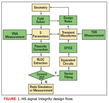
Figure 1 shows a typical high-speed signal integrity design flow1.
One of the important goals here is to generate design rules. The 2D
field solver software is used to determine rules for board stack-up,
impedance, trace width and spacing. Simulation predicts delay and
crosstalk. There is a certain amount of overhead required for
simulation, i.e., obtaining and verifying simulation models, careful
setup and rigorous interpretation of the results by signal integrity
engineers, etc. The tools in this flow can be used many times in the
design of a PCB. The user needs to be well versed in signal integrity
concepts, cause and effect, and interpretation of the analysis. In
addition, the time to run this flow can be significantly long.

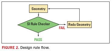
In contrast, Figure 2
shows the design rule program flow – it is very simple, easy to
configure, and with a very short learning (and re-learning) curve. The
program has a short run time, and the user need not be a signal
integrity expert. As companies may send PCB designs to other areas of
the world for their fabrication, this flow would be used by a designer
during the layout process and before a formal design review in order to
avoid major rework.

The following examples show how a
design rule checker works. The database was created in Cadence Allegro,
and the Design Rule Checker is IBM’s EMSAT EMC rule checker, configured
as an SI rule checker.

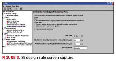
Figure 3
shows the SI design rules on the left side, with the options used to
configure a critical net. Since this rule can vary between internal and
external layers, there are two user definable “distance to the edge of
the plane” thresholds. Note that the rules can be turned on
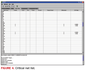
individually. The rules using a green bullet will be run. Next, the
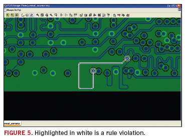
critical nets are identified (Figure 4). That’s it – run the check. If there are any violations, both a text report and a graphical view are generated. Figure 5 shows one such violation. The offending net is highlighted, showing a segment that is too close to the edge of the plane.


One
of the great features of a rule checker is that it eliminates human
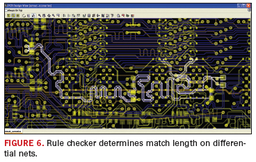
error. Consider trying to match the lengths of these two differential
nets manually (Figure 6). Differential routing is
prevalent in today’s designs, and one of the major concerns in DDR
design is the relative skew between the nets in the bus. SI simulation
is performed to generate physical rules for the router. The nets are
then routed to ensure that net lengths are within a specified tolerance
of each other. To verify that the design meets the requirements, simply
let the design rule determine that these two traces differ in length by
235 mils, which may or may not be acceptable for design requirements.
Such a requirement can be entered as a threshold, and the output of the
rule checker displays this information as a simple pass/fail.

Should
there be any violations, a design rule checker allows viewing of the
violation location by quickly zooming in and highlighting the
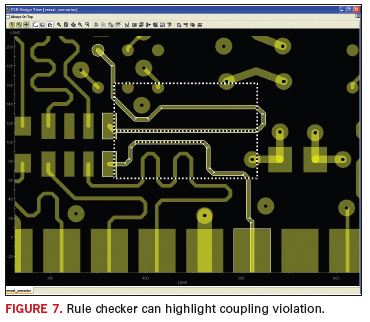
net/trace/via/component that violated the specific rule. Figure 7
shows a coupling violation that could cause excessive crosstalk. Note
that the coupled segment is highlighted, and a bounding box encloses
the violation.

Conclusion
In
general, design rule checkers can be used for a wide variety of PCB
constraints such as impedance control, impedance discontinuities, loss,
reflections, termination, traces crossing splits2, etc. Dr. Eric Bogatin describes over one hundred general design guidelines to minimize signal integrity problems3.
Typical high speed PCBs have many constraints and very dense routing,
and it is likely that not all the design rules will be met. It is then
up to the engineer to see if the violations require redesign. Rapid
identification and the viewing of any violations allow this decision to
be made quickly.
No one tool that can do everything.
In the SI analysis of PCBs, different tools of varying complexity can
be used: for example, a field solver, complex full wave analysis,
transmission line simulation, etc. Each tool has its own function and
value. Post route design rule checkers offer easy to use, configurable,
and quick verification of PCB design, ensuring that design guidelines
determined by a time-consuming simulation analysis have been followed. PCD&F
Guy de Burgh is a signal integrity and EMC consultant; This email address is being protected from spambots. You need JavaScript enabled to view it.. Gene Garat is in sales with MossBay EDA; This email address is being protected from spambots. You need JavaScript enabled to view it..
REFERENCES
1. Ching-Chao Huang, Signal Integrity Modeling and Simulation Tools, DesignCon 2004.
2. Abe Riazi, “Effects of Plane Splits on High–Speed Signals, Part 1,” Printed Circuit Design & Manufacture, Feb. 2007.
3. Eric Bogatin, Signal Integrity – Simplified, Appendix A.


