In RF designs, it’s important to identify and correct circuit
interactions as the system design evolves to reduce cycle time and
prevent unnecessary re-spins.
Today, RF (radio frequency) circuitry is sneaking into more and more
products. As this happens, more designers are faced with allowing RF
circuitry to share board space with other technologies such as
high-speed digital and analog circuits.
The combination of RF and non-RF circuitry in close proximity can cause
a lot of pain to design teams. Multiple design iterations and very long
design times are common. Traditional design techniques have not been
very helpful as they typically focus on RF alone and don’t consider the
interactions of the complete system.
In this article, we will take a practical look at modern RF design in
the context of a complete system and see how careful planning and
design can significantly improve the success rate, as well as shorten
design times.
RF design can be painful, especially so when seen in the context of
system design. Why is that? In the past, RF was typically isolated
modules – boards with solely RF content. Today, we combine all kinds of
technology on the same dense board, and as dimensions are constantly
shrinking, the risk of interaction between technologies, such as
high-speed digital and RF, increases.
Currently, this interaction cannot fully be avoided. We are typically
not able to design out all interactions but are instead faced with
designing a system with interaction but not more than the circuit can
accept and still perform as intended. With this in mind, we can
identify three areas of interest (each topic could fill a book or more):
Design methodology. How to best design a mixed-technology product.
Circuit interaction. How to manage the interaction between modules of different technologies.
Verification. How to verify and validate a mixed-technology design.
Design Methodology
Today’s methodologies go back over 10 years when RF design was a
different ball game. In the classic flow, the RF designer is a
contributor of technology that eventually will end up on a circuit
board. The RF modules are designed in a dedicated RF design solution
and, when ready, transferred to the system PCB layout using design
translation.
The benefit of this method is that the designer can focus on the RF by
itself, not bothered by non-RF issues, and there are cases where this
is a real advantage. The downside is that the RF engineer can’t see the
impact he may cause or what will be affected by other circuits, and he
stays as a contributor while the desired situation, in this case, is a
team player role.
For multi-technology designs, much can be gained in a methodology where
all technologies can be co-designed in a manner where everyone is a
team player rather than module contributors. By providing a
collaborative environment, concurrent design teams can design their
technology in parallel while being aware of what is being designed by
other teams, thus eliminating some re-spins.
Circuit Interaction
Multi-technology design is about circuits living in harmony. You avoid
being a noisy neighbor, and you don’t walk in your neighbor’s garden.
The issue is that the circuits are becoming noisier. Plus, they are
placed closer together than in the past … a trend that will continue no
matter what.
Hence, circuits do impact each other, and the challenge is to manage
how and how much so the circuits still perform as specified. There are
several areas impacting the interaction; the most obvious one is parts
placement. Unfortunately, parts placement is not free since everything
has to fit, and each technology has specific placement requirements.
Unwanted Coupling
We also have to deal with unwanted coupling. Unwanted coupling is any
coupling of energy from one system to another where it is not
intentionally designed as a part of the circuit.
There are several sources or “entries” for unwanted coupling: the most
obvious path is direct coupling in the form of inductive and capacitive
coupling between signal conductors. Today, it is commonly understood
that wide traces at narrow spacing far from ground will have large
mutual capacitance and inductance and, hence, be able to couple energy
between them. Since this is obvious, it becomes second nature to
control this direct coupling.
The really nasty and sneaky scoundrel is indirect coupling from the
power/ground system, and signal return paths. In a circuit schematic,
we only draw the signal paths, and the return path is implicit.
Everyone knows that a return path is needed, or the circuit remains
open and will not work. You don’t typically wire them as you do with
signal conductors. They appear indirectly as a consequence of your
wiring and the design of your power/ground system. The smart thing
about return paths is that the circuit will find one if one exists, or
we would have an open circuit. The bad thing is that if this return
path is not where you want it to be, you can (most likely will!) get
into trouble.
This means that, to be successful, we must change from “indirect”
creation of return paths to actively considering return paths in the
design work. For every routed signal, we have to ensure that we have a
proper return path that is located where we want it and that we don’t
obstruct already created paths, because signals sharing a part of the
return path have common impedance coupling (energy coupled from one
signal to the other).
The larger the area spanned by signal and return path, the larger the
radiation and susceptibility. (EMI is proportional to the loop area.)
Where is the Return Path?
At DC, the return path is a straight line (path of least resistance),
but as frequency increases, we cannot simplify and just say “the path
of least resistance” anymore. It is in fact the path of least
impedance. At the low to medium-high frequency of the digital
high-speed spectrum, inductance is the dominating part of impedance.
Therefore, we can somewhat simply say that the return path is the path
of least inductance.
In today’s circuit boards, this path is usually in the ground plane
right under the signal conductor. This deviates only if there are
obstacles in the form of a slotted or split ground plane or where vias
perforate the ground plane enough to cut the return path.
At RF frequencies (this includes ultra-high-speed digital), capacitance
becomes dominant. Thus, the signal will typically find its return path
as the path of least capacitance. This makes things extremely
complicated as the path of “least capacitance” is not as predicable as
for inductance. It may very well include any conductive surface in
proximity, such as shield boxes or a metal cabinet. At the same time,
the return path is really critical to circuit function. We need to
establish where the path is and that it is not shared for two sensitive
signals to avoid common impedance coupling between them.
The key to controlling indirect coupling is proper grounding.
Obviously, we don’t want RF and digital (or analog) to share return
paths. This is why we work with separate grounds. Connecting all ground
in a single point helps ensure that the return paths are not shared
between the systems. However, within the same ground system, we need to
manage the return paths - keeping in mind the rule that it will be the
path of least impedance for the frequency with which we are working.
Power Feed Leaks
Return path and separate grounding helps, but in an RF system, we also
need to ensure that RF energy must not leak onto the power supply
itself and radiate or cause other problems there.
When I started doing RF design, we used closed metal cabinets for each
module, with each cabinet carefully grounded. We used so-called
feed-through capacitors for every signal or power entering or leaving
the shielded compartment. This was a conductor with a coaxial
capacitance to ground intended to short circuit any RF energy trying to
escape. We also used RF chokes made of a quarter-wavelength of wire
wound as a coil. Connected in a series with power or LF lines, they
acted as a high-impedance obstacle to further limit RF leaks.
Today, this is too cumbersome of an approach, and integrated board
compartments are more practical replacements. We still need to decouple
interconnects very carefully to prevent RF leaks via power and
low-frequency lines in the design.
Ground Fences
In RF system designs, we frequently see each module in the design
encapsulated by a narrow ground guard stitched with via holes: either a
single row of vias or a dual staggered row. When designers are asked
why they use a certain via spacing or pattern, the answer often
includes wind direction and shoe size. Luckily, some work has been
published on this topic; so there is no reason to resort to black magic.
We can use via fencing for both power lines and signal lines. As we all
know, currents in power planes are overlaid with transients. This can
make the power bus radiate the same way as a microstrip patch antenna1.
Xin Wu et al. suggest that setting the via spacing in the fence to less
than 1/10th wave length can give up to 25 dB suppression compared to no
fencing
1.
You would think that the closer a via fence is placed to an RF line the
better. However, when placed too close, the radiation losses increase.
This will actually increase the coupling
2. As a rule of thumb, the via
fence must be set away from the RF trace by at least four times the
distance between the signal layer and the ground layer of a multilayer
PCB
2.
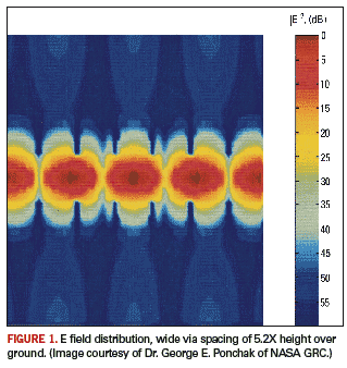
Figure 1 shows the field distribution for a stripline with widely
spaced via fencing. The vias are 1X height over ground away from the
strip line, and the via spacing is 5.2X height over ground. The
radiation losses are clearly visible.
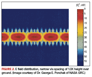
 Figure 2
 shows the same strip with a much narrower via spacing of 1.3X
height over ground. The radiation losses are significantly lower here.
Dr. Ponchak (recommended reading on this topic!) suggests that the
smaller the via spacing, the better
2. A solid wall would be ideal if it
could be manufactured.

In RF systems, we also need to manage the ground and power planes. We
have already covered that the currents on these planes have a transient
component and that transient currents through a conductor mean
radiation, which we obviously don’t want. This leads us to via
peppering of power/ground planes. Again, we have an area ruled by
“black magic;” “This is what we’ve always done so it must be good …”
Still, there are some published papers that can help us better
understand what really happens to the power and ground planes.
If we inject a current between two parallel plates, they will radiate
due to something called parallel plate excitation that allows signals
to propagate between the plates. Trust me, if the “parallel plates” are
your ground plane, you will want to suppress this. Typically, we have
multiple ground layers, and we pepper the ground areas and stitch the
edges of ground areas with vias to short the planes together preventing
this propagation mode in the ground plane.
3Interestingly, via array acts as band pass filters at high frequencies.
The via to via spacing controls the pass band poles, and we will soon
see that the via-to-via spacing is very important
4.
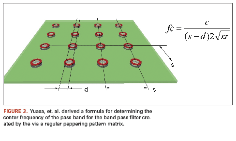
Takeshi Yuasa et al. have found the pass band frequency to be as shown
in
Figure 3 where εr is the relative permittivity of the dielectric
material, and c is the speed of light, a function of via diameter, via
spacing and dielectric material
3. However, this calculated frequency is
not the same as the usable upper limit!

The space enclosed by four via holes forms a cavity, which will
resonate at about 0.65X the center frequency (Fc)
3. This becomes the
real upper limit. At resonance, the grounding effect of the via array
is lost, and the structure will no longer prevent the parallel plate
mode excitation. From this, it is clear that how we arrange the vias,
their diameter and their pitch is important, and does impact the
effectiveness of the via fencing and via peppering.
Verification
In a classic RF design flow, RF modules are simulated in the RF design
environment (initially), not taking into account the actual PCB
implementation. Verification includes repeating that simulation, but
now with all known PCB features included, such as surrounding non-RF
signals, metal planes and shapes, via stitching, via peppering and
other techniques. Ideally, the differences in simulation results are
negligible, but the reality is that serious issues are always found.
The tool integrations of the traditional flow make it very cumbersome
to set up and run this type of simulation with incremental updates
while the circuit design and layout are in progress. Typically, Gerber,
DXF or GDS-II files are used, which means that all design intent is
lost in the interface due to primitive data formats.
New methodologies combined with new design tools that use a more
elegant integration, where design data keeps its “intelligence,” make
it possible to keep the intent of the design and run repeated
simulations very quickly.
This makes it possible to quickly identify problems caused by circuit
interaction and correct them as you go along in a “correct by design”
flow. Interactions will happen. Identifying and correcting these
interactions as the system design evolves, rather than in the end,
offers the potential to yield much shorter design cycles and fewer of
those cycles. This is because the earlier the issues can be identified,
the easier they can be corrected. Making substantial changes to a dense
and complete design can take a very long time.
PCD&FPer Viklund is director of IC packaging & RF with Mentor Graphics, Systems Design Division;
This email address is being protected from spambots. You need JavaScript enabled to view it..
REFERENCES
1. Wu, Xin, Mahammad H. Ke~mani and Omar M. Ramahi. ”Mitigating
Multilayer PCB Power Bus Radiation Through Novel Mesh Fencing
Techniques,” Mechanical Engineering Department, Electrical and Computer
Engineering Department, and CALCE Electronic Products and Systems
Center, University of Maryland College Park, MD.
2. Ponchak, George E., Donghoon Chen, Jong-Gwan Yook, and Linda P. B.
Katehi. ”Characterization of Plated Via Hole Fences for Isolation
Between Stripline Circuits in LTCC Packages,” IEEE THIF61.
3. Yuasa, Takeshi, Tamotsu Nishino, and Hideyuki Oh-hashi. ”Simple
Design Formula for Parallel Plate Mode Suppression by Ground
Via-Holes,” Mitsubishi Electric Corp., 5-1-1 Ofuna, Kamakura, Kanagawa,
247-8501 Japan.
4. Tischler, Thorsten, Matthias Rudolph, Andreas Kilk, and Wolfgang
Heinrich. ”Via Arrays for Grounding in Multilayer Packaging Frequency
Limits and Design Rules, Ferdinand-Braun-Institut für
Höchstfrequenztechnik (FBH), D-12489 Berlin, Germany.


