A successful DfM program is part methodology, part design environment
and part toolset, with a foundation based on fabrication
processes.
If you’re an engineer designing electronics systems for anything other
than pure R&D bench work, this is what you do: design, redesign,
simulate and, ultimately, manufacture your product – all while
balancing the many sets of simultaneous constraints (target component
costs, form/fit/finish, compliance, complexity, reliability, etc.) to
deliver a robust, innovative and profitable project.
DfM (design for manufacture) is about creating the detailed
documentation necessary to deliver accurate, easily reproducible end
products. DfM is also about hitting the center of your allowed process
windows so a process deviation doesn’t end up ruining your yield.
DfM has been an active, ongoing topic of discussion in other
CAD/EDA
sectors, such as semiconductor design. In a recent industry white
paper, semiconductor software firm Synopsys (Mountain View, CA) made
the following observations: “Design for manufacturing is about
connections … connections within the design flow; connections within
the manufacturing flow; and, most importantly, connections between
design and manufacturing. These connections are required to address
fundamental issues associated with yield loss in today’s leading-edge …
products and are key to a robust DfM solution.”
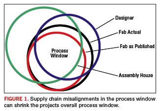
Figure 1 illustrates
the point: each step in the design and manufacture of your project has
a process window. Your project’s ultimate process window for DfM
purposes is the intersection of all the process windows in your design
flow.

Design for Manufacture: Where It Fits in the Design Flow
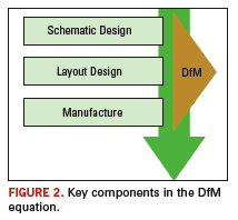
Historically, implementing a DfM protocol for your design team has been
a largely human endeavor, built up from expert knowledge, practical
understanding and a collaborative engineering culture (
Figure 2). While
the human portion of DfM persists, it is no longer sufficient.

PCB design tools have been available on the market almost since the
dawn of the
CAD/EDA industry. Exactly when PCB design rule check
(DRC) and DfM tools emerged onto the marketplace differs depending upon
which tools you include, but the general consensus is that DRC/DfM
checkers for PCBs were available by the late 1980s. This begs the
question: if DfM has been around so long, why the sudden spotlight?
Perhaps the answer lies in the culmination of ever-increasing design
complexities, shorter design cycles and the increased levels of
outsourcing for design and manufacture that have created the
“compelling event” for DfM. Therefore, DfM is part methodology, part
design environment and part toolset. In other words, successful DfM is
influenced by the workflow process being followed. The realization is
that a true DfM solution must be holistic; it must include the design
team, manufacturing supply chain, and test and component suppliers all
together in a single design and manufacture ecosystem. This is exactly
where traditional PCB DfM systems go astray; these systems miss the
opportunity to make meaningful design flow connections.
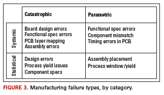
The intent of DfM is to help engineers prevent or minimize the yield
issues before they materialize. It’s easy to summarize sub-categories
of failures and their likely place of occurrence. Manufacturing yield
issues can be categorized into four combinations (
Figure 3):

Catastrophic vs. Parametric
- Catastrophic – board design is non-functional
- Parametric – board functions, but doesn’t perform to specification.
Systemic vs. Statistical
- Systemic – functionality does not work as planned in a consistent and reproducible way
- Statistical – failures are seemingly random or do not correlate to another condition.
The Standalone Conundrum
Throughout the process of writing this article, a common opinion
emerged that the standalone PCB DfM tools currently in wide
availability work more like pre-engineering design validation tools
than they do as an interactive resource for in-design decision-making.
Given the pricing for these standalone DfM tools, it’s also clear that
software companies are not aiming to sell their tools to the typical
designer. Depending on features and installations, some standalone
ftools can run as much as $100,000 – an amount that many firms are
simply unable to absorb.
“The current tools are thorough, but not all that helpful to the
overall design flow,” says Joe Zaccari, vice president at
Stilwell-Baker, when asked about the current state of PCB DfM. “You
don’t get a lot of value from a tool that just tells you what you did
wrong after the design is completed. It is much more efficient to work
with ongoing feedback. We get better design results, higher yields and
shorter design cycles when we can engage a customer using interactive
methods.”
This leaves standalone DfM tool developers in a lurch: the tool’s high
cost means that the overall target market is limited to
well-capitalized companies with enough PCB fabrication volume to
justify the expense – PCB fabrication shops. Because the market niche
is so narrow, PCB DfM standalone tool developers are required to charge
a lot for their tools to cover the expense of creating them. In fact,
some PCB fabricators have begun offering to run low- or no-cost DfM on
anyone’s design, with the expectation that the customer will then place
the order with the fabricator and help defray the cost of operating the
DfM tool in the first place.
The Next Stage in DfM Evolution: Web-Based Tools
Wisely, some vendors are developing DfM tools that target the end user.
Generally speaking, these tools are taking a web-based service
application service provider approach, such as the Free DfM service
from Advanced Circuits or the recently announced Control Center XP from
UK-based fabricators Direct Logix and Artetch Circuits. A web-based
model has its advantages such as easy distribution of bug fixes and the
potential to be software-independent. However, it falls short on its
ability to integrate tightly into the design flow, particularly when
users interact with the tool by submitting their designs to the service
via e-mail or website, and the DfM service responds by e-mailing a
report containing the DfM issues identified. “They’ve got the idea
right, but the implementation is wrong,” says Stilwell-Baker’s Zaccari
of the web-based tools. “This is like e-mailing your word document to a
spell checker service so you can get a list of misspelled words in
under an hour. It is extremely inefficient as it requires redesign of
the board for reasons that should have been known upfront.”
CAD Tools: A Simple Solution Often Overlooked
In an e-mail interview, Ed Rodledo, general manager of CadSoft USA, the
US subsidiary of CadSoft GmBH, and maker of Eagle PCB Layout said,
“There is another way. Use the DRC engine already built into your
CAD
system. Any commercial-grade design tool will have a DRC/DfM engine
built in. Define the manufacturing rules there, and design
interactively to the DfM restrictions published by your fab of choice.”
Robledo seems to have company with this thinking. “A number of
CAD
tools support the concept of DRC or DfM rules files,” says Nancy Viter,
customer service manager at Sunstone Circuits, picking up on Robledo’s
point. “It’s a feature of the tool that’s built in and commonly
overlooked in the prototype phase. Design engineers don’t often have
full knowledge of either the process rule specifics, nor the DRC
engine’s rules syntax. Some engineers tell us they’ve given up on the
interactive DRC checks because their best efforts to write a rule deck
only resulted in a long list of spurious errors. Instead of designing
boards, they find themselves in an endless debugging loop in order to
get meaningful DRC results.”
Robledo’s and Viter’s comments are echoed by PCB engineers elsewhere in
the industry. “Writing rule decks is not my preferred activity,” says
John Draut, director of hardware design at LightFleet in Camas, WA. “I
have multiple vendors with differing rules, and I’m not the one who
knows all the subtleties of a particular fabricator’s process. Though I
often use the rules checker inside the layout tool, I can’t be certain
that the rule settings are applicable to the specific fabrication
vendor. Last minute fabrication vendor decisions can have significant
impact on my development schedule thanks to differing rules,” says
Draut. “So interactive rules checking with multiple ‘vendor certified’
rule decks to choose from during PCB layout would significantly improve
the development schedule when compared to batch mode checks run at the
fab vendor’s facility.”
CAD tool vendors, perhaps understandably, are reluctant to take on the
task of writing rule decks. Their
core competence is in software
development, not process definition. Lee Harding, engineering manager
at Sunstone Circuits, finds: “There are dozens of popular or
semi-popular PCB design layout tools and something like 350 PCB
manufacturing companies in North America alone. If a
CAD tool company
were to try to support many or most of the fabricators, the task would
be huge. That’s why they don’t do it.” Harding adds, “The same holds
true for fabricators. They haven’t seen the value in taking the time to
write rule decks for all the
CAD tools in the field. Most fabricators
prefer to receive Gerber files and not interact with the
CAD tools that
make the Gerbers.”
Table 1 examines the strengths and weaknesses of the different DfM tool approaches.
The Sunstone Approach
Sunstone Circuits is pursuing the DfM rule deck approach, collaborating
with PCB software developers to create DRC/DfM rule decks that
accurately and completely implement Sunstone’s design rules. Once
completed, tested and certified, Sunstone makes these rule decks freely
available from its website, and partnering websites. Designers planning
to use Sunstone for PCB fabrication can load these rule decks into
their
CAD systems and design direct to Sunstone’s manufacturing
processes. The payoff can be tremendous for designers.
“If they’ve got a DRC rule deck they can depend on, our designers are
more likely to use denser layouts and really pack in the geometries,
even during prototype,” said Stilwell-Baker’s Zaccari, speaking of his
highly experienced staff. “That offers fewer design iterations to our
customers, shortening their time to market and increasing our overall
value-add to the project.”
With a certified rule deck driving the
CAD tool’s routing constraints,
engineers can concentrate instead on other aspects of their design that
are equally key to DfM, such as parts research or thermal effects. “It
can have a big effect,” responded Duane Benson, of Screaming Circuits
when asked about the impact of DfM on downstream PCB manufacturing
services, such as assembly. “Physical spacing between the components,
for example, is frequently overlooked by automated DRC in the
CAD
package. Yet, something that looks good on the board, such as putting
several components with large thermal mass close together, can make an
otherwise good design unmanufacturable.”
Benson’s comments illustrate the point that there is a lot more to DfM
than the normal route spacing, footprints, drill sizes or thermal
issues. Component choices also affect the manufacturability of a
design. If a completed design uses a component, for example, that is
discontinued by the manufacturer shortly thereafter, the design team
will certainly be going through another revision just to accommodate
that part’s obsolescence. This is yet another set of tradeoffs
designers must make during the design process.
Conclusion
As tools continue to develop, we can expect that DfM’s current
boundaries will expand to more sophisticated checks, possibly even
bringing part-specific lifecycle information into the design process in
new and innovative ways. This thought leads us full circle to what PCB
designers do: innovate. Talk to a PCB designer about his work, and
you’ll be reminded that the job is all about making tradeoffs:
balancing densities with heat buildup; trading square inches for
components; and achieving the same performance with lower cost
components. With all these balancing decisions, any room in the
prototype phase a designer can capitalize upon to truly experiment with
an alternate design approach that could result in a major innovation is
valuable.
“If the designer is confident in the design rules, then he or she may
have the extra bandwidth to try some alternative approaches alongside
the tried-and-true ones,” comments Harding. “If our no-cost DfM/DRCs
leave more engineering budget available for experimentation, then
perhaps we help promote some innovation.”
PCD&F
Nolan Johnson is
CAD/EDA product marketing manager at Sunstone;
This email address is being protected from spambots. You need JavaScript enabled to view it..


